Publications
(PDF
files are provided)
Journal
Papers:
2025
350. S.-R. Kim, Y. Zhan, N. Davis, S. Bellamkonda, L. Gillan, E. Hakola, J. Hiltunen, A. Javey, "Electrodermal activity as a proxy for sweat rate monitoring during physical and mental activities", Nature Electronics, 8, 353–361, 2025.
349.
W. Kim, K. Lee, S. Choi, E. Park, G. Kim, J. Ha, Y. Kim, J. Jang, J. H.
Oh, H. Kim, W. Jiang, J. Yoo, T. Kim, Y. Kim, K.-N. Kim, J. Hong, A.
Javey, D.-w. Rha, T.-W. Lee, K. Kang, G. Wang, C. Park, "Electrochemiluminescent tactile visual synapse enabling in situ health monitoring", Nature Materials, 2025, https://doi.org/10.1038/s41563-025-02124-x
348.
Y. Shi, P. P. Roy, N. Higashitarumizu, T.-Y. Lee, Q.
Li, A. Javey, K. Landfester, I. McCulloch, G. R. Fleming, "Annihilation-limited long-range exciton transport in high-mobility conjugated copolymer films", Proceedings of the National Academy of Sciences, 122 (17), e2413850122, 2025.
347.
I.K.M. R. Rahman, T. Kim, I. Kim, N. Higashitarumizu, S. Wang, S. Wang,
H. M. Kim, J. Bullock, V. Altoe, J. W. Ager III, D. C. Chrzan, A.
Javey, "Thermally Stable Ruthenium Contact for Robust p-Type Tellurium Transistors", Nano Letters, 25 (10), 3956-3963, 2025.
346. M. Alawein, J. W. Ager, A. Javey, D. C. Chrzan, "Strain-induced lateral heterostructures: Hole localization and the emergence of flat bands in rippled MoS2 monolayers", Physical Review Materials, 9 (2), L021002, 2025.
345.
J. Geng, D. Zhang, I. Kim, H. M. Kim, N. Higashitarumizu, I. K. M. R.
Rahman, L. Lam, J. W. Ager III, A. V. Davydov, S. Krylyuk and A. Javey,
"Unusually Strong Near-Infrared Photoluminescence of Highly Transparent Bulk InSe Flakes", Advanced Functional Materials, 35 (3), 2413672, 2025.
2024
344.
K. Lee, N. Higashitarumizu, S. Wang, C. Kim, C. Y. Ho, J. W. Oh, G.
Zan, M. Madsen, T.-W. Lee, D. C. Chrzan, C. Park, A. Javey, "Meter-scale van der Waals films manufactured via one-step roll printing", Science Advances 10 (36), eadq0655, 2024.
343. Y. Cai, Z. Wang, J. Wan, J. Li, R. Guo, J.W. Ager, A. Javey, H. Zheng, J. Jiang, J. Wu, "Ion diffusion retarded by diverging chemical susceptibility", Nature Communications, 15 (1), 5814, 2024.
342. N. Davis, J. Heikenfeld, C. Milla, A. Javey, "The challenges and promise of sweat sensing", Nature Biotechnology, 42, 860–871, 2024.
341. I. Kim, N. Higashitarumizu, IKM R. Rahman, S. Wang, H. M. Kim, J. Geng, R. R. Prabhakar, J. W. Ager III, A. Javey, "Low Contact Resistance WSe2 p-Type Transistors with Highly Stable, CMOS-Compatible Dopants", Nano Letters, 24 (43), 13528-13533, 2024.
340. N. Higashitarumizu, S. Wang, S. Wang, H. Kim, J. Bullock, A. Javey, "Black Phosphorus for Mid-Infrared Optoelectronics: Photophysics, Scalable Processing, and Device Applications", Nano Letters, 24 (42), 13107-13117, 2024.
339.
J. I. Kim, N. Higashitarumizu, S. Wang, R. Yalisove, M. C. Scott, S. Y.
Song, A. Javey, "Multicolor Inks of Black Phosphorus for
Midwave‐Infrared Optoelectronics", Advanced Materials, 2402922, 2024.
338.
J. Li, R. Yang, N. Higashitarumizu, S. Dai, J. Wu, A. Javey, C. P.
Grigoropoulos, "Transient Nanoscopy of Exciton Dynamics in 2D
Transition Metal Dichalcogenides", Advanced Materials, 36 (21), 2311568, 2024.
337. H. Sun, O. Sahin, A. Javey, J. W. Ager, D. C. Chrzan, "Theory of mechanical exfoliation of van der Waals bonded layered materials", Physical Review Materials, 8, 064003, 2024.
336. N.
Higashitarumizu, T. Kawashima, T. Smart, R. Yalisove, C. Y. Ho, M.
Madsen, D. C. Chrzan, M. C. Scott, R. Jeanloz, H. Yusa, A. Javey,
"Mid-Infrared, Optically Active Black Phosphorus Thin Films on
Centimeter Scale", Nano Letters, 10, 3104-3111, 2024.
335.
S. Wang, N. Higashitarumizu, B. Sari, M. C. Scott, A. Javey,
"Quantitative Mid-infrared Photoluminescence Characterization of Black
Phosphorus–Arsenic Alloys", ACS Nano, 18, 5907–5914, 2024.
2023
334. N. Gupta, S. Wang, N. Higashitarumizu, V. Wang, K. Lee, C. Park, A. Javey, "Large-scale efficient mid-wave infrared optoelectronics based on black phosphorus ink", Science Advances, 9, eadi9384, 2023.
333. N. Higashitarumizu, S. Tajima, J. Kim, M. Cai, A. Javey, "Long operating lifetime mid-infrared LEDs based on black phosphorus", Nature Communications, 14, 4845, 2023.
332. V. Wang, S. Z. Uddin, J. Park, A. Javey, "Highly
multicolored light emitting arrays for compressive spectroscopy", Science
Advances, 9, eadg1607, 2023.
331. N.
Higashitarumizu, S. Z. Uddin, D. Weinberg, N. S. Azar, I. K. M. R. Rahman, V.
Wang, K. B. Crozier, E. Rabani, A. Javey, “Anomalous thickness dependence of
photoluminescence quantum yield in black phosphorous”, Nature Nanotechnology, 18 (5), 507-513, 2023.
330. J. Li, K. Dong, T. Zhang, D. Tseng, C.
Fang, R. Guo, J. Li, Y. Xu, C. Dun, J. J. Urban, T. Hong, C. P.
Grigoropoulos, A. Javey, J. Yao, J. Wu, "Printable, emissivity-adaptive and albedo-optimized covering for year-round energy saving", Joule, 7 (11), 2552-2567, 2023.
329. I. K. M. R. Rahman, S. Z. Uddin, M. Yeh, N. Higashitarumizu, J. Kim, Q. Li, H. Lee, J. W. Ager III, A. Javey, "Gate Controlled Excitonic Emission in Quantum Dot Thin Films", Nano Letters, 23, 10164–10170, 2023.
328.V. Wang, Q. Lin, A. Javey, "Electrically driven light emission from single quantum dots using pulsed MOS capacitors", Applied Physics Letters, 123, 131108, 2023.
327. J. Kim, V. Wang, S. C. Kim, J. Y. Lee, A. Javey, "A Color-Tunable Alternating Current Organic Light Emitting Capacitor", Nano Letters, 23, 12, 5822–5827, 2023.
326. B. Sari, S. E. Zeltmann, C. Zhao, P. M. Pelz, A. Javey, A. M. Minor, C. Ophus, M. C. Scott, "Analysis of Strain and Defects in Tellurium-WSe2 Moiré Heterostructures Using Scanning Nanodiffraction", ACS Nano, 17, 22326–22333, 2023.
325. A. Aggarwal, M. Dautta, L. F. Ayala-Cardona, A. Wudaru, A. Javey, "Wearable Humidity Sensor for Continuous Sweat Rate Monitoring", Advanced Materials Technologies, 8, 2300385, 2023.
324.
S. Balendhran, M. Taha, S. Wang, W. Yan, N. Higashitarumizu, D. Wen, N.
Sefidmooye Azar, J. Bullock, P. Mulvaney, A. Javey, K. B. Crozier, "Flexible Vanadium Dioxide Photodetectors for Visible to Longwave Infrared Detection at Room Temperature", Advanced Functional Materials, 33, 2301790, 2023.
323.
A. G. S. Vilasam, S. Adhikari, B. Gupta, S. Balendhran, N.
Higashitarumizu, J. Tournet, L. Li, A. Javey, K. B. Crozier, S.
Karuturi, C. Jagadish, H. H. Tan, "Large-area
epitaxial growth of InAs nanowires and thin films on hexagonal boron
nitride by metal organic chemical vapor deposition", Nanotechnology, 34 (49), 495601, 2023.
322. Kaichen Dong, Jiachen Li, Tiancheng Zhang, Fangda Gu,
Yuhang Cai, Niharika Gupta, Kechao Tang, Ali Javey, Jie Yao, Junqiao
Wu, "Single-pixel reconstructive mid-infrared micro-spectrometer",
Optics Express, 31, 9, 14367-14376, 2023.
321. G. H. Ahn, A. D.
White, H. Kim, N. Higashitarumizu, F. M. Mayor, J. F. Herrmann, W. Jiang, K. K.S.
Multani, A. H. Safavi-Naeini, A. Javey, J. Vučković, “Platform-agnostic
waveguide integration of high-speed photodetectors with evaporated tellurium
thin films”, Optica, 10, 3, 349-355, 2023.
320. Y. Luo, et al, “Technology Roadmap for Flexible Sensors”, ACS Nano, 17, 6, 5211–5295, 2023.
319. J. M. Buriak, et al, “Best
Practices for Using AI When Writing Scientific Manuscripts: Caution, Care, and
Consideration: Creative Science Depends on It”, ACS Nano, 17, 5,
4091–4093, 2023.
318. T. Schenkel, A. M. Snijders, K. Nakamura, P. A. Seidl, B.
Mak, L. Obst-Huebl, H. Knobel, I. Pong, A. Persaud, J. van Tilborg, T.
Ostermayr, S. Steinke, E. A. Blakely, Q. Ji, A. Javey, R. Kapadia, C. G. R.
Geddes, E. Esarey, “Carbon nanotube substrates enhance SARS-CoV-2 spike protein
ion yields in matrix-assisted laser desorption–ionization mass spectrometry”, Applied
Physics Letters, 122, 050601, 2023.
317. M. Dautta, L. F. Ayala‐Cardona, N. Davis, A. Aggarwal, J.
Park, S. Wang, L. Gillan, E. Jansson, M. Hietala, H. Ko, J. Hiltunen, A. Javey,
“Tape‐Free, Digital Wearable Band for Exercise Sweat Rate Monitoring”, Advanced
Materials Technologies, 8, 2201187, 2023.
2022
316. I. K. M. R. Rahman, S. Z. Uddin, H. Kim, N. Higashitarumizu, A. Javey, "Low voltage AC electroluminescence in silicon MOS capacitors", Applied Physics Letters, 121 (19), 193502, 2022.
315. N. Gupta, H. Kim, N.S. Azar, S.Z. Uddin, D.-H. Lien, K.B. Crozier, A.
Javey, “Bright Mid-Wave Infrared Resonant-Cavity Light-Emitting Diodes
Based on Black Phosphorus”, Nano Letters, 22 (3), 1294-1301, 2022.
314. S. Z. Uddin, N. Higashitarumizu, H. Kim, I.K.M.R. Rahman, A. Javey, “Efficiency Roll-Off Free Electroluminescence from Monolayer WSe2”, Nano Letters, 22, 5316–5321, 2022.
313. H. Batiz, J. Guo, G.H. Ahn, H. Kim, A. Javey, J.W. Ager III, D.C. Chrzan, “Theory of liquid-mediated strain release in two-dimensional materials”, Physical Review Materials, 6 (5), 054005, 2022.
312. S.Z. Uddin, N. Higashitarumizu, H. Kim, J. Yi, X. Zhang, D. Chrzan, A. Javey, “Enhanced Neutral Exciton Diffusion in Monolayer WS2 by Exciton-Exciton Annihilation”, ACS Nano, 16 (5), 8005-8011, 2022.
311. M. Bariya, N. Davis, L. Gillan, E. Jansson, A. Kokkonen, C. McCaffrey, J. Hiltunen, A. Javey, “Resettable Microfluidics for Broad-Range and Prolonged Sweat Rate Sensing”, ACS Sensors, 7 (4), 1156-1164, 2022.
310. C. Zhao, H. Batiz, B. Yasar, W. Ji, M.C. Scott, D.C. Chrzan, A. Javey, “Orientated Growth of Ultrathin Tellurium by van der Waals Epitaxy”, Advanced Materials Interfaces, 9 (5), 2101540, 2022.
309. S.Z. Uddin, N. Higashitarumizu, H. Kim, E. Rabani, A. Javey, “Engineering Exciton Recombination Pathways in Bilayer WSe2 for Bright Luminescence”, ACS Nano, 16 (1), 1339-1345, 2022.
308. B.
Sari, H. Batiz, C. Zhao, A. Javey, D.C. Chrzan, M.C. Scott, “Structural
heterogeneity in non-crystalline TexSe1-x thin films”, Applied Physics
Letters, 121, 012101, 2022.
307. Y. Rho, H. Kim, A. Javey, C.P. Grigoropoulos, “Laser‐Assisted Thermomechanical Thinning of MoTe2 in Nanoscale Lateral Resolution”, Advanced Materials Interfaces, 9 (23), 2200634, 2022.
2021
306.
H. Kim, S. Z. Uddin, D.-H. Lien, M. Yeh, N. S. Azar, S. Balendhran, T.
Kim, N. Gupta, Y. Rho, C. P. Grigoropoulos, K. B. Crozier, A. Javey, "Actively variable spectrum optoelectronics with black phosphorus", Nature, 596, 232–237, 2021.
305. H. Kim, S. Z. Uddin, N. Higashitarumizu, E. Rabani, A. Javey, "Inhibited nonradiative decay at all exciton densities in monolayer semiconductors", Science, 373, 448, 2021.
304. K. Tang, K. Dong, J. Li, M. P. Gordon, F. G. Reichertz, H. Kim, Y.
Rho, Q. Wang, C.-Y. Lin, C. P. Grigoropoulos, A. Javey, J. J. Urban, J.
Yao, R. Levinson, J. Wu, "Temperature-adaptive radiative coating for all-season household thermal regulation", Science, 374, 1504–1509, 2021.
303. H. Y. Y. Nyein, M. Bariya, B. Tran, C. H. Ahn, B. J. Brown, W. Ji, N. Davis, A. Javey, "A wearable patch for continuous analysis of thermoregulatory sweat at rest", Nature Communications, 12, 1823, 2021.
302. V. Wang, A. Javey, "A Resonantly Driven, Electroluminescent Metal Oxide Semiconductor Capacitor with High Power Efficiency", ACS Nano, 15, 9, 15210–15217, 2021.
301. C. Zhao, H. Batiz, B. Yasar, H. Kim, W. Ji, M. C. Scott, D. C. Chrzan, A. Javey. "Tellurium Single‐Crystal Arrays by Low‐Temperature Evaporation and Crystallization", Advanced Materials, 33 (37), 2100860, 2021.
300. S. Balendhran, Z. Hussain, V. R. Shrestha, J. Cadusch, M. Ye, N.
S. Azar, H. Kim, R. Ramanathan, J. Bullock, A. Javey, V. Bansal, K. B.
Crozier, "Copper
Tetracyanoquinodimethane (CuTCNQ): A Metal–Organic Semiconductor for
Room-Temperature Visible to Long-Wave Infrared Photodetection", ACS Applied Materials & Interfaces, 13 (32), 38544-38552, 2021.
299. N. S. Azar, J. Bullock, S. Balendhran, H. Kim, A. Javey, K. B. Crozier, "Light–Matter Interaction Enhancement in Anisotropic 2D Black Phosphorus via Polarization-Tailoring Nano-Optics", ACS Photonics, 8, 1120-1128, 2021.
298. Y. Lin, M. Bariya, A. Javey, "Wearable Biosensors for Body Computing", Advanced Functional Materials, 31 (39), 2170290, 2021.
297. N. S. Azar, J. Bullock, V. R. Shrestha, S. Balendhran, W. Yan, H. Kim, A. Javey, K. B. Crozier, "Long-Wave Infrared Photodetectors Based on 2D Platinum Diselenide atop Optical Cavity Substrates", ACS Nano, 15, 6573-6581, 2021.
296. S. Z. Uddin, E. Rabani, A. Javey, "Universal Inverse Scaling of Exciton−Exciton Annihilation Coefficient with Exciton Lifetime", Nano Letters, 21, 424–429, 2021.
295. V. Wang, Y. Zhao, A. Javey, "Performance Limits of an Alternating Current Electroluminescent Device", Advanced Materials, 33 (2), 2005635, 2021.
294. J. Zhao, H. Y. Y. Nyein, L. Hou, Y. Lin, M. Bariya, C. H. Ahn, W. Ji, Z. Fan, A. Javey, "A Wearable Nutrition Tracker", Advanced Materials, 33 (1), 2006444, 2021.
2020
293. Y. Zhao, V. Wang, D.-H. Lien, A. Javey, "A generic electroluminescent device for emission from infrared to ultraviolet wavelengths", Nature Electronics, 3, 612–621, 2020.
292. L. Gu, S. Poddar, Y. Lin, Z. Long, D. Zhang, Q. Zhang, L. Shu, X. Qiu,
M. Kam, A. Javey, Z. Fan, "A biomimetic eye with a hemispherical
perovskite nanowire array retina", Nature, 581, 278–282, 2020.
291. C. Zhao, C. Tan, D.-H. Lien, X. Song, M. Amani, M. Hettick, H. Y. Y. Nyein, Z. Yuan, L. Li, M. C. Scott, A. Javey, "Evaporated tellurium thin films for p-type field-effect transistors and circuits", Nature Nanotechnology, 15, 53–58, 2020. (additional article in news & views)
290. M. Hettick, H. Li, D.-H. Lien, M. Yeh, T.-Y. Yang, M. Amani, N. Gupta, D. C. Chrzan, Y.-L. Chueh, A. Javey, "Shape-controlled single-crystal growth of InP at low temperatures down to 220 °C", Proceedings of the National Academy of Sciences (PNAS), 117 (2) 902-906, 2020.
289. M. Bariya, L. Li, R. Ghattamaneni, C. H. Ahn, H. Y. Y. Nyein, L.-C. Tai, A. Javey, "Glove-based sensors for multimodal monitoring of natural sweat", Science Advances, 6, 35, eabb8308, 2020.
288. Y. Zhao, V. Wang, A. Javey, "Molecular Materials with Short Radiative Lifetime for High-Speed Light-Emitting Devices", Matter, 3 (6), 1832-1844, 2020.
287. S. Z. Uddin, H. Kim, M. Lorenzon, M. Yeh, D.-H.
Lien, E. S. Barnard, H. Htoon, A. Weber-Bargioni, A. Javey,
"Neutral Exciton Diffusion in Monolayer MoS2", ACS Nano, 14, 13433–13440, 2020.
286.
D. W. Gardner, Y. Xia, H. M. Fahad, A. Javey, C. Carraro, R. Maboudian,
"Improved Hydrogen Sensitivity and Selectivity in PdO with
Metal-Organic Framework Membrane", Journal of the Electrochemical Society, 167, 147503, 2020.
285.
C. Tan, M. Amani, C. Zhao, M. Hettick, X. Song, D.‐H. Lien, H. Li, M.
Yeh, V. R. Shrestha, K. B. Crozier, M. C. Scott, A. Javey, "Evaporated SexTe1‐x Thin Films with Tunable Bandgaps for Short‐Wave Infrared Photodetectors", Advanced Materials, 32, 2001329, 2020.
284. H. Liu, X. Yu, K. Wu, Y. Gao, S. Tongay, A. Javey, L. Chen, J. Hong, J. Wu, "Extreme in-plane thermal conductivity anisotropy in titanium trisulfide caused by heat-carrying optical phonons", Nano Letters, 20, 5221–5227, 2020.
283. A. J. Goodman, D.-H. Lien, G. H. Ahn, L. L. Spiegel, M. Amani, A. P. Willard, A. Javey, W. A. Tisdale, "Substrate-Dependent Exciton Diffusion and Annihilation in Chemically Treated MoS2 and WS2", The Journal of Physical Chemistry C, 124, 12175–12184, 2020.
282. L.-C. Tai, C. H. Ahn, H. Y. Y. Nyein, W. Ji, M. Bariya, Y. Lin, L. Li, A. Javey, "Nicotine Monitoring with Wearable Sweat Band", ACS Sensors, 5, 1831–1837, 2020.
281. Z. Yuan, M. Bariya, H. M. Fahad, J. Wu, R. Han, N. Gupta, A.
Javey, "Trace‐Level, Multi‐Gas Detection for Food Quality Assessment
Based on Decorated Silicon Transistor Arrays", Advanced Materials, 1908385, 2020.
280. W. Ji, T. Allen, X. Yang, G. Zeng, S. De Wolf, A. Javey, "Polymeric Electron-Selective Contact for Crystalline Silicon Solar Cells with an Efficiency Exceeding 19%", ACS Energy Letters, 5, 897-902, 2020.
279. J. Cho, M. Amani, D.‐H. Lien, H. Kim, M. Yeh, V. Wang, C. Tan, A. Javey, "Centimeter‐Scale and Visible Wavelength Monolayer Light‐Emitting Devices", Advanced Functional Materials, 1907941, 2019.
278. Y. Yu, H. Y. Y. Nyein, W. Gao, A. Javey, "Flexible Electrochemical Bioelectronics: The Rise of In Situ Bioanalysis", Advanced Materials, 1902083, 2019.
277.
J. Sun, A. Sapkota, H. Park, P. Wesley, Y. Jung, B. B. Maskey, Y. Kim,
Y. Majima, J. Ding, J. Ouyang, C. Guo, J. Lefebvre, Z. Li, P. R. L.
Malenfant, A. Javey, G. Cho, "Fully R2R‐Printed Carbon‐Nanotube‐Based
Limitless Length of Flexible Active‐Matrix for Electrophoretic Display
Application", Advanced Electronic Materials, 6(4), 1901431, 2020.
276. H. Liu, C. Yang, B. Wei, L. Jin, A. Alatas, A. Said, S. Tongay, F.
Yang, A. Javey, J. Hong, J. Wu, "Anomalously Suppressed Thermal
Conduction by Electron‐Phonon Coupling in Charge‐Density‐Wave Tantalum
Disulfide", Advanced Science, 1902071, 2020.
275. C. Zhao, L. Hurtado, A. Javey, "Thermal stability for Te-based devices", Appl. Phys. Lett. 117, 192104, 2020.
274. V. R. Shrestha, B. Craig, J. Meng, J. Bullock, A. Javey, K. B.
Crozier, "Mid-to long-wave infrared computational spectroscopy with a
graphene metasurface modulator", Scientific Reports, 10, 5377, 2020.
273. H. Taz, B. Prasad, Y.-L. Huang, Z. Chen, S.-L. Hsu, R. Xu, V.
Thakare, T. S. Sakthivel, C. Liu, M. Hettick, R. Mukherjee, S. Seal, L.
W. Martin, A. Javey, G. Duscher, R. Ramesh, R. Kalyanaraman, "Integration of amorphous ferromagnetic oxides with multiferroic materials for room temperature magnetoelectric spintronics", Scientific Reports, 10, 3583, 2020.
2019
272. D.-H. Lien, S. Z. Uddin, M. Yeh, M. Amani, H. Kim, J. W. Ager III,
E.
Yablonovitch, and A. Javey, "Electrical
suppression of all nonradiative
recombination pathways in monolayer semiconductors", Science, 364, 468–471, 2019.
271.
H. Y. Y. Nyein,
M. Bariya, L. Kivimäki,
S. Uusitalo, T. S. Liaw, Elina Jansson,
C. H. Ahn, J. A. Hangasky, J. Zhao, Y. Lin,
T. Happonen, M. Chao, C. Liedert,
Y. Zhao, L.-C. Tai, J. Hiltunen,
A. Javey, "Regional
and Correlative Sweat Analysis Using High-throughput Microfluidic
Sensing
Patches Towards Decoding Sweat", Science Advances, 5 (8), eaaw9906, 2019.
270. T. Allen, J. Bullock, X. Yang, A. Javey, S. De
Wolf, "Passivating contacts unlock the full potential of silicon solar
cells", Nature Energy, 4, 914–928, 2019.
269.
H. Zhao, Y. Zhao, Y. Song, M. Zhou, W. Lv, L. Tao, Y. Feng, B. Song, Y.
Ma, J. Zhang, J. Xiao, Y. Wang, D.-H. Lien, M. Amani, H. Kim, X. Chen,
Z. Wu, Z. Ni, P. Wang, Y. Shi, H. Ma, X. Zhang, J.-B. Xu, A. Troisi, A.
Javey, X. Wang, "Strong optical response and light emission from a monolayer molecular crystal", Nature Communications, 10, 5589, 2019.
268. H. Kim, G. H. Ahn,
J. Cho, M. Amani, J. P. Mastandrea, C. K. Groschner, D.-H. Lien, Y.
Zhao, J. W. Ager III, M. C. Scott, D. C. Chrzan, A. Javey, "Synthetic
WSe2 monolayers with high photoluminescence quantum yield",
Science Advances,
5, eaau4728, 2019.
267. S. B. Desai, H. M. Fahad, T. Lundberg, G. Pitner, H. Kim, D. Chrzan,
H.-S. P. Wong, A. Javey, "Gate Quantum Capacitance Effects in Nanoscale
Transistors", Nano Letters, 19, 7130-7137, 2019.
266. P. Zhao, R. Wang, D.-H. Lien, Y. Zhao, H. Kim, J. Cho, G. H. Ahn,
A. Javey, "Scanning Probe Lithography Patterning of Monolayer
Semiconductors and Its Application for Quantifying Edge Recombination",
Advanced Materials, 31, 1900136, 2019.
265. Z. Yuan, L. Hou, M. Bariya, H. Y. Y. Nyein, L.-C. Tai, W. Ji, L. Li, A. Javey, " A Multi-Modal Sweat Sensing Patch for Cross-Verification of Sweat Rate, Total Ionic Charge, and Na+ Concentration", Lab on a Chip, 19, 3179 - 3189, 2019.
264. L.-C. Tai, T.
S. Liaw, Y. Lin, H. Y. Y. Nyein, M. Bariya, W. Ji, M. Hettick, C. Zhao,
J. Zhao, L. Hou, Z. Yuan, Z. Fan, A. Javey, "A Wearable Sweat Band for Noninvasive Levodopa Monitoring", Nano Letters, 19, 6346-6351, 2019.
263.
W. Ji, Y. Zhao, H. M. Fahad, J. Bullock, T. Allen, D.-H. Lien, S. De
Wolf, A. Javey, "Dip
Coating Passivation of Crystalline Silicon by Lewis Acids", ACS Nano, 13, 3723−3729, 2019.
262. N. Gupta, H. M. Fahad, M. Amani, X. Song, M. Scott, A. Javey, "Elimination
of Response to Relative Humidity Changes in Chemical-Sensitive Field
Effect Transistors", ACS
Sensors, 4, 1857-1863, 2019.
261.
J. Bullock, Y. Wan, M. Hettick, X. Zhaoran, S. P. Phang, D. Yan, H.
Wang, W. Ji, C. Samundsett, Z. Hameiri, D. Macdonald, A. Cuevas, A.
Javey, "Dopant-Free
Partial Rear Contacts Enabling 23% Silicon Solar Cells", Advanced Energy Materials, 1803367,
2019.
260. J. Zhao, Y. Lin, J. Wu, H. Y. Y. Nyein, M. Bariya, L.-C. Tai, M.
Chao, W. Ji, G. Zhang, Z. Fan, A. Javey, "A Fully Integrated and
Self-Powered Smartwatch for Continuous Sweat Glucose Monitoring", ACS Sensors, 4, 1925-1933, 2019.
259.
Y. Lin, M. Bariya, H. Y. Y. Nyein, L. Kivimäki, S. Uusitalo, E.
Jansson, W. Ji, Z. Yuan, T. Happonen, C. Liedert, J. Hiltunen, Z. Fan,
A. Javey, "Porous
Enzymatic Membrane for Nanotextured Glucose Sweat Sensors with High
Stability toward Reliable Noninvasive Health Monitoring", Advanced Functional Materials,
29, 1902521, 2019.
258. J. Pak, I. Lee, K. Cho, J.-K. Kim, H. Jeong, W.-T. Hwang, G. H. Ahn, K. Kang, W. J. Yu, A. Javey, S. Chung, T. Lee, "Intrinsic Optoelectronic Characteristics of MoS2 Phototransistors via a Fully Transparent van der Waals Heterostructure", ACS Nano, 13, 9638-9646, 2019.
257. K.Takei, W. Gao, C. Wang, A. Javey, "Physical and
Chemical Sensing With Electronic Skin", Proceedings of IEEE, 107, 2155-2167, 2019.
256. D. Zhang, L. Gu, Q. Zhang, Y. Lin, D.-H. Lien, M. Kam, S. Poddar,
E.
Garnett, A. Javey, Z. Fan, "Increasing
photoluminescence quantum
yield by nanophotonic design of quantum-confined halide perovskite
nanowire arrays", Nano Letters,
19, 2850-2857, 2019.
255. W. Gao, H. Ota, D. Kiriya, K. Takei, A. Javey, "Flexible
Electronics toward Wearable Sensing", Accounts of Chemical Research, 52,
523−533, 2019.
254. G. Gurudayal, J. W. Beeman, J. Bullock, H. Wang, J. Eichhorn, C.
M. Towle, A. Javey, F. M. Toma, N. Mathews, J. W. Ager III, "Si Photocathode with Ag-Supported
Dendritic Cu Catalyst for CO2 Reduction", Energy & Environmental Science,
12, 1068-1077, 2019.
253. D. W. Gardner, X. Gao, H. M. Fahad, A.-T. Yang, S. He, A. Javey,
C. Carraro, R. Maboudian, "Transistor‐based
work function measurement of metal‐organic frameworks for
ultra‐low‐power, rationally designed chemical sensors", Chemistry–A European Journal, 25 (57), 13176-13183, 2019.
252. K. Han, G. H. Ahn, J. Cho, D.-H. Lien, M. Amani, S. B. Desai, G.
Zhang, H. Kim, N. Gupta, A. Javey, M. C. Wu, "Bright electroluminescence in
ambient conditions from WSe2 p-n diodes using pulsed
injection", Applied Physics
Letters, 115, 011103, 2019.
251. G. Zhang, M. Amani, A. Chaturvedi, C. Tan, J. Bullock, X. Song, H.
Kim, D.-H. Lien, M. C. Scott, H. Zhang, A. Javey, "Optical and electrical properties of
two-dimensional palladium diselenide", Applied Physics Letters, 114,
253102, 2019.
250. V. Nguyen, H. Gramling, C. Towle, W. Li, D.-H. Lien, H. Kim, D. C. Chrzan, A. Javey, K. Xu, J. Ager, H. Taylor. "Deterministic assembly of arrays of lithographically defined WS2 and MoS2 monolayer features directly from multilayer sources into van der Waals heterostructures", Journal of Micro and Nano-Manufacturing, 7(4), 041006.
249. Y. Zeng, S. Khandelwal, K. F. Shariar, Z. Wang, G. Lin, Q. Cheng,
P. Cui, R. Opila, G. Balakrishnan, S. Addamane, P. Taheri, D. Kiriya,
M. Hettick, A. Javey, "InAs
FinFETs Performance Enhancement by
Superacid Surface Treatment", IEEE
Transactions on Electron Devices, 66, 1856 - 1861, 2019.
248. H. M. Gramling, C. M. Towle, S. B. Desai, H. Sun, E. C. Lewis, V.
D. Nguyen, J. W. Ager, D. Chrzan, E. M. Yeatman, A. Javey, H. Taylor,
"Spatially
precise transfer of patterned monolayer WS2 and MoS2
with features larger than 104 μm2 directly from
multilayer sources", ACS Applied
Electronic Materials, 1 (3), 407–416, 2019.
247. H. Ali, S. Koul, G. Gregory, J. Bullock, A. Javey, A. Kushima, K.
O. Davis, "In Situ Transmission Electron
Microscopy Study of Molybdenum
Oxide Contacts for Silicon Solar Cells", physica status solidi (a), 216,
1800998, 2019.
2018
246.
J. Bullock, M. Amani, J. Cho, Y.-Z. Chen, G. H. Ahn, V. Adinolfi, V. R.
Shrestha, Y. Gao, K. B. Crozier, Y.-L. Chueh, A. Javey, "Polarization-resolved
black phosphorus/molybdenum disulfide mid-wave infrared photodiodes
with high detectivity at room temperature", Nature Photonics, 12, 601–607, 2018.
245. M. Bariya, H. Y. Y. Nyein, A. Javey, "Wearable
Sweat Sensors", Nature
Electronics, 1, 160–171, 2018.
244. D.-H.
Lien, M. Amani, S. B. Desai, G. H. Ahn, K. Han, J.-H. He, J. W. Ager
III, M. C. Wu, A. Javey, "Large-area
and bright pulsed
electroluminescence in monolayer semiconductors", Nature Communications, 9, 1229,
2018.
243.
M.
Bariya, Z. Shahpar, H. Park, J. Sun, Y. Jung, W. Gao, H. Y. Y. Nyein,
T. S. Liaw, L.-C. Tai, Q. P. Ngo, M. Chao, Y. Zhao, M. Hettick, G. Cho,
A. Javey, "Roll-to-Roll
Gravure Printed Electrochemical Sensors for Wearable and Medical Devices",
ACS Nano,
12, 6978–6987, 2018.
242. H. Y. Y. Nyein, L.-C. Tai, Q. P. Ngo, M. Chao, G.
Zhang, W. Gao,
M.
Bariya, J. Bullock, H. Kim, H. M. Fahad, A. Javey, "A Wearable
Microfluidic Sensing Patch for Dynamic Sweat Secretion Analysis", ACS Sensors, 3, 944-952, 2018.
241.
L.-C. Tai, W. Gao, M. Chao, M. Bariya, Q. P. Ngo, Z. Shahpar, H. Y. Y.
Nyein, H. Park, J. Sun, Y. Jung, E. Wu, H. M. Fahad, D.-H. Lien, H.
Ota, G. Cho, A. Javey, "Methylxanthine drug
monitoring with wearable
sweat sensors", Advanced
Materials, 30, 1707442, 2018.
240.
H. M. Fahad, N. Gupta, R. Han, S. B. Desai, A. Javey, "Highly Sensitive
Bulk Silicon Chemical Sensors with Sub-5 Nanometer Thin Charge
Inversion
Layers", ACS Nano, 12
(3), 2948–2954, 2018.
239.
James Bullock, Yimao Wan, Zhaoran Xu, Stephanie Essig, Mark Hettick,
Hanchen Wang, Wenbo Ji, Mathieu Boccard, Andres Cuevas, Christophe
Ballif, Ali Javey, "Stable
Dopant-Free Asymmetric Heterocontact Silicon
Solar Cells with Efficiencies Above 20%", ACS Energy Letters, 3, 508–513,
2018.
238.
M.
Amani, C. Tan, G. Zhang, C. Zhao, J. Bullock, X. Song, H. Kim, V. R.
Shrestha, Y. Gao, K. B. Crozier, M. Scott, A. Javey, "Solution-Synthesized High-Mobility
Tellurium Nanoflakes for Short-Wave Infrared Photodetectors", ACS Nano, 12 (7), 7253–7263, 2018.
237. M. S. Eggleston, S. B. Desai, K. Messer, S. A. Fortuna, S. R.
Madhvapathy, J. Xiao, X. Zhang, E. Yablonovitch, A. Javey, M. C. Wu, "Ultra-Fast Spontaneous
Emission from a Slot-Antenna Coupled WSe2 Monolayer", ACS Photonics, 5 (7), 2701–2705,
2018.
236. C. M. Sutter-Fella, Q. P. Ngo, N. Cefarin, K. Gardener,
N. Tamura,
C.
V. Stan, W. S. Drisdell, A. Javey, F. M. Toma, I. D Sharp, "Cation-Dependent
Light-Induced Halide Demixing in Hybrid Organic-Inorganic Perovskites",
Nano Letters,
18, 3473-3480, 2018.
235.
Y. Wan, J. Bullock, M. Hettick, Z. Xu, C. Samundsett, D. Yan, J. Peng,
A. Javey, A. Cuevas, "Temperature
and Humidity Stable Alkali/Alkaline‐Earth Metal Carbonates as Electron
Heterocontacts for Silicon Photovoltaics", Advanced Energy Materials, 1800743,
2018.
234. Y. Wan, J. Bullock, M. Hettick, Z. Xu, D. Yan, J. Peng, A. Javey,
A. Cuevas, "Zirconium oxide
surface passivation of crystalline silicon", Applied Physics Letters, 112 (20),
201604, 2018.
233. G. Conti, S. Nemsak, C.-T. Kuo, M. Gehlmann, C. Conlon,
A. Keqi,
A. Rattanachata, O. Karslıoğlu, J. Mueller, J. Sethian, H. Bluhm, J. E.
Rault, J. P. Rueff, H. Fang, A. Javey, and C. S. Fadley, “Characterization of free
standing InAs quantum membranes by standing wave hard x-ray
photoemission spectroscopy", APL
Materials, 6, 058101, 2018.
232. D. Yoo, Y. Kim, M.
Min, G. H. Ahn, D.-H. Lien, J. Jang, H. Jeong, Y. Song, S. Chung, A.
Javey, T. Lee, "Highly
reliable superhydrophobic protection for organic field-effect
transistors by fluoroalkylsilane-coated TiO2 nanoparticles",
ACS Nano,
12, 11062-11069, 2018.
231. B. Cheng, T.-Y. Li, P. Maity, P.-C. Wei, D. Nordlund,
K.-T. Ho,
D.-H. Lien, C.-H. Lin, R.-Z. Liang, X. Miao, I. A. Ajia, J. Yin, D.
Sokaras, A. Javey, I. S. Roqan, O. F. Mohammed, J.-H. He, "Extremely reduced
dielectric confinement in two-dimensional hybrid perovskites with large
polar organics", Communications
Physics, 1, 80, 2018.
230. H. Ali, S. Koul, G. Gregory, J. Bullock, A. Javey, A. Kushima, K.
O. Davis, "Thermal Stability of
Hole-Selective Tungsten Oxide: In Situ Transmission Electron Microscopy
Study", Scientific Reports,
8, 12651, 2018.
2017
229. H. M. Fahad, H.
Shiraki, M. Amani, C. Zhang, V. S.
Hebbar, W. Gao,
H. Ota, M. Hettick, D. Kiriya, Y.-Z. Chen, Y.-L. Chueh, A. Javey. "Room
temperature multiplexed gas sensing using chemical sensitive 3.5 nm
thin silicon transistors", Science
Advances, 3, e1602557, 2017.
228. J. H. Park, A.
Sanne, Y. Guo, M. Amani, K. Zhang, H. C.P. Movva, J. A.
Robinson, A. Javey, J. Robertson, S. K. Banerjee, A. C. Kummel, "Defect
passivation of transition metal dichalcogenides via a charge transfer
van der Waals interface" Science
Advances, 3 (10), e1701661, 2017.
227.
G. H. Ahn, M. Amani, H. Rasool, D.-H. Lien, J. P. Mastandrea, J. W.
Ager, M. Dubey, D. C. Chrzan, A. M. Minor, A. Javey.
"Strain-engineered
growth of two-dimensional materials", Nature Communications, 8, 608, 2017.
226. S. Emaminejad, W.
Gao, E. Wu, Z. A. Davies, H. Y. Y. Nyein, S. Challa, S. P. Ryan, H. M.
Fahad, K. Chen, Z. Shahpar, S. Talebi, C. Milla, A. Javey, R. W. Davis.
"Autonomous
sweat extraction and analysis applied to cystic fibrosis and glucose
monitoring using a fully integrated wearable platform", Proceedings of the National Academy of
Sciences, 114, 4625-4630, 2017.
225. Y. Gao, H. Ota, E. W. Schaler, K. Chen, A. Zhao, W. Gao, H. M.
Fahad, Y. Leng, A. Zheng, F. Xiong, C. Zhang, L.-C. Tai, P. Zhao, R. S.
Fearing, A. Javey. "Wearable
Microfluidic Diaphragm Pressure Sensor for Health and Tactile Touch
Monitoring", Advanced Materials,
1701985, 2017.
224. H. Ota, M. Chao, Y.
Gao,
E. Wu, L.-C. Tai, K. Chen, Y. Matsuoka, K.
Iwai, H. M. Fahad, W. Gao,
H. Y. Y. Nyein, L. Lin, A. Javey. "3D Printed Earable Smart
Devices for Real-time Detection of
Core Body Temperature", ACS
Sensors, 2 (7), 990–997, 2017.
223.
Y. Wan, S. K. Karuturi, C. Samundsett, J. Bullock, M. Hettick, D. Yan,
J. Peng, P. R. Narangari, S. Mokkapati, H. H. Tan, C. Jagadish, A.
Javey, A. Cuevas, "Tantalum
Oxide Electron-Selective Heterocontacts for
Silicon Photovoltaics and Photoelectrochemical Water Reduction", ACS Energy Letters, 3
(1), 125–131, 2017.
222.
M. Amani, E. Regan, J. Bullock, G. H. Ahn, A. Javey. "Mid-Wave Infrared
Photoconductors Based on Black Phosphorous-Arsenic Alloys", ACS Nano, 11 (11), 11724–11731,
2017.
221. A. B. Sachid, S. B. Desai, A. Javey, C. Hu. "High-Gain Monolithic 3D CMOS
Inverter using Layered Semiconductors", Applied Physics Letters, 111,
222101, 2017.
220.
Gurudayal, J. Bullock, D. F. Srank�, C. M. Towle, Y. Lum, M. Hettick,
A. Javey, J. Ager, "Efficient
solar-driven electrochemical CO2 reduction to hydrocarbons
and oxygenates", Energy &
Environmental Science, 10, 2222-2230, 2017.
219.
Xiaojie Xu, Sudhanshu Shukla, Ya Liu, Binbin Yue, James Bullock,
Longxing Su, Yanmei Li, Ali Javey, Xiaosheng Fang, Joel W Ager, "Solution‐Processed
Transparent Self‐Powered p‐CuS‐ZnS/n‐ZnO UV Photodiode", Phys. Status Solidi RRL, 1700381,
2017.
218.
N. Grant, T. Niewelt, N. Wilson, E. Wheeler-Jones, J. Bullock, M.
Al-Amin, M. Schubert, A. van Veen, A. Javey, J. Murphy,
"Superacid-Treated Silicon
Surfaces: Extending the Limit of Carrier
Lifetime for Photovoltaic Applications", IEEE Journal of Photovoltaics, 7,
1574-1583, 2017.
217.
J. Bullock, H. Ota, H. Wang, Z. Xu, M. Hettick, D. Yan, C. Samundsett,
Y. Wan, S. Essig, M. Morales-Masis, A. Cuevas, A. Javey. "Microchannel
contacting of crystalline silicon solar cells", Scientific Reports,
7, 9085, 2017.
216. P. Zhao, M. Amani, D.-H. Lien, G. H. Ahn, D. Kiriya, J. P.
Mastandrea, J. W. Ager III, E. Yablonovitch, D. C. Chrzan, A. Javey, "Measuring the Edge Recombination Velocity
of Monolayer Semiconductors", Nano
Letters, 17, 5356–5360, 2017.
215. P. Taheri, H. M.
Fahad, M. Tosun, M. Hettick, D. Kiriya, K. Chen, A. Javey, "Nanoscale Junction Formation by
Gas-Phase Monolayer Doping", ACS
Applied Materials & Interfaces, 9 (24), 20648-20655, 2017.
214. H.
Kim, D.-H. Lien, M. Amani, J. W. Ager, A. Javey,
"Highly Stable Near-Unity
Photoluminescence Yield in Monolayer MoS2 by Fluoropolymer
Encapsulation and Superacid Treatment", ACS Nano, 11 (5), 5179-5185, 2017.
213.W. S. Drisdell, L. Leppert, C. M. Sutter-Fella, Y.
Liang, Y. Li, Q. P. Ngo, L. F. Wan, S. Gul, T. Kroll, D. Sokaras, A.
Javey, J. Yano, J. B. Neaton, F. M. Toma, D. Prendergast, I. D. Sharp, "Determining
Atomic-Scale Structure and Composition of Organo-Lead Halide
Perovskites by Combining High-Resolution X-ray Absorption Spectroscopy
and First-Principles Calculations", ACS
Energy Letters, 2 (5), 1183-1189,
2017.
212. H. Ko, A. Javey. "Smart
Actuators and Adhesives for Reconfigurable Matter", Accounts of Chemical Research, 50
(4), 691-702, 2017.
211. Y. Wan, C. Samundsett, J. Bullock, M. Hettick, T. Allen, D. Yan,
J. Peng, Y. Wu, J. Cui, A. Javey, A. Cuevas. "Conductive and Stable Magnesium
Oxide Electron‐Selective Contacts for Efficient Silicon Solar Cells",
Advanced
Energy Materials, 7, 1601863, 2017.
210. C. M. Sutter-Fella, D. W. Miller, Q. P. Ngo, E. T. Roe, F. M.
Toma, I. D. Sharp, M. C. Lonergan, A. Javey. "Band
Tailing and Deep Defect States in CH3NH3Pb (I1-xBrx)3
Perovskites as Revealed by Sub-Bandgap Photocurrent", ACS Energy Letters, 2 (3), 709–715, 2017.
209.
T.-Y. Kim, Y. Song, K. Cho, M. Amani, G. H. Ahn, J.-K. Kim, J. Pak, S.
Chung, A. Javey, T. Lee, "Analysis of
the interface characteristics of
CVD-grown monolayer MoS2 by noise measurements", Nanotechnology, 28 (14), 145702,
2017.
208.
H. Medina, J.-G. Li, T.-Y. Su, Y.-W. Lan, S.-H. Lee, C.-W. Chen, Y.-Z.
Chen, A. Manikandan, S.-H. Tsai, A. Navabi, X. Zhu, Y.-C. Shih, W.-S.
Lin, J.-H. Yang, S. R. Thomas, B.-W. Wu, C.-H. Shen, J.-M. Shieh, H.-N.
Lin, A. Javey, K. L. Wang, and Y.-L. Chueh. “Wafer-Scale Growth of
WSe2 Monolayers Toward Phase-Engineered Hybrid WOx/WSe2
Films with Sub-ppb NOx Gas Sensing by a Low-Temperature
Plasma-Assisted Selenization Process”, Chemistry of Materials, 29 (4),
1587–1598, 2017.
207. T. G. Allen, J. Bullock, Q. Jeangros, C. Samundsett, Y. Wan, J.
Cui, A. Hessler‐Wyser, S. De Wolf, A. Javey, A. Cuevas. "A Low Resistance Calcium/Reduced
Titania Passivated Contact for High Efficiency Crystalline Silicon
Solar Cells", Advanced Energy
Materials, 1602606, 2017.
206. T. G. Allen, J. Bullock, P. Zheng, B. Vaughan, M. Barr,
Y. Wan, C.
Samundsett, A. Javey, A. Cuevas, "Calcium
contacts to n-type
crystalline silicon solar cells", Progress
in Photovoltaics: Research and Applications, 25, 636-644, 2017.
2016
205. S. B. Desai, S. R.
Madhvapathy, A. B. Sachid, J. P. Llinas, Q.
Wang, G. H. Ahn, G. Pitner, M. J. Kim, J. Bokor, C. Hu, H.-S. P. Wong,
A. Javey, "MoS2
transistors with 1-nanometer gate lengths", Science, 354, 99-102, 2016.
204. W. Gao, S. Emaminejad, H. Y. Y. Nyein, S. Challa, K. Chen, A.
Peck, H. M. Fahad, H. Ota, H. Shiraki, D. Kiriya,
D.-H. Lien, G. A. Brooks, R. W. Davis, A. Javey. "Fully-integrated wearable sensor arrays
for multiplexed in-situ
perspiration analysis", Nature,
529, 509–514, 2016.
203. J. Bullock, M. Hettick, J. Geissbühler, A. J. Ong, T. Allen,
C. M. Sutter-Fella, T. Chen, H. Ota, E. W.
Schaler, S. De Wolf, C. Ballif, A. Cuevas, A. Javey, "Efficient silicon solar cells
with dopant-free asymmetric heterocontacts", Nature Energy, 15031, 2016.
202. K. Chen, R. Kapadia, A. Harker, S. Desai, J. S. Kang, S. Chuang,
M. Tosun, C. M. Sutter-Fella, M. Tsang, Y. Zeng, D. Kiriya, J. Hazra,
S. R. Madhvapathy, M. Hettick, Y.-Z. Chen, J. Mastandrea, M. Amani, S.
Cabrini, Y.-L. Chueh, J. W. Ager III, D. C. Chrzan, A. Javey. "Direct growth of single
crystalline III-V semiconductors on amorphous substrates", Nature Communications, 7, 10502,
2016.
201. Y. Li,
J. K. Cooper, W. Liu, C. M. Sutter-Fella, M. Amani, J. W. Beeman, A.
Javey, J. W. Ager, Y. Liu, F. M. Toma,
I. D. Sharp. "Defective
TiO2 with high photoconductive gain for efficient and stable
planar heterojunction perovskite solar cells", Nature
Communications, 7, 12446, 2016.
200. J. Bullock, D. Kiriya, N. E Grant, A. Azcatl, M. Hettick, T. Kho,
P. Phang, H. C. Sio, D. Yan, D. MacDonald, M. A. Quevedo-Lopez, R. M.
Wallace, A. Cuevas, A. Javey. "Superacid
passivation of crystalline silicon surfaces", ACS Applied Materials & Interfaces,
8, 24205–24211, 2016.
199. H. Y.
Y. Nyein, W. Gao, Z. Shahpar, S. Emaminejad, S. Challa, K. Chen, H. M.
Fahad, L.-C. Tai, H. Ota, R. W. Davis, A. Javey. "A Wearable
Electrochemical Platform for Non-Invasive Simultaneous Monitoring of Ca2+
and pH", ACS Nano, 10, 7216–7224, 2016.
198. M. Amani, R. A. Burke, X.
Ji, P. Zhao, D.-H. Lien, P. Taheri, G. H. Ahn, D. Kirya, J. W. Ager
III,
E. Yablonovitch, J. Kong, M. Dubey, A. Javey. "High Luminescence Efficiency in MoS2
Grown by Chemical Vapor Deposition", ACS Nano, 10, 6535–6541, 2016.
197. D. Kiriya, P. Lobaccaro, H. Nyein, P. Taheri, M. Hettick,
H. Shiraki, C. M. Sutter-Fella, P. Zhao, W. Gao, R. Maboudian, J. Ager,
A. Javey. "General Thermal
Texturization Process of MoS2 for Efficient Electrocatalytic
Hydrogen Evolution Reaction", Nano Letters, 16, 4047–4053, 2016.
196.
J. Bullock, P. Zheng, Q. Jeangros, M. Tosun, M.
Hettick, C. M. Sutter-Fella, Y. Wan, T. Allen, D. Yan, D. Macdonald,
S. De Wolf, A. Hessler-Wyser, A. Cuevas, A. Javey, "Lithium Fluoride Based Electron
Contacts for High Efficiency n-type Crystalline Silicon Solar Cells",
Advanced Energy Materials, 1600241, 2016.
195. Y. Wan,
C. Samundsett, J. Bullock, T. Allen, M. Hettick, D. Yan, P. Zheng, X.
Zhang, J. Cui, J. A. McKeon, A. Javey, A. Cuevas. "Magnesium fluoride
electron–selective contacts for crystalline silicon solar cells", ACS
Applied Materials & Interfaces, 8, 14671–14677, 2016.
194. W. Gao,
H. Y. Y. Nyein, Z. Shahpar, H. M. Fahad, K. Chen, S. Emaminejad, Y.
Gao, L.-C.
Tai, H. Ota, E. Wu, J. Bullock, Y. Zeng, D.-H. Lien, A. Javey, "Wearable
Microsensor Array for Multiplexed Heavy Metal Monitoring of Body Fluids",
ACS Sensors, 1, 866–874, 2016. (ACS Editors'
Choice; Cover Article)
193. M. Amani, P. Taheri, R. Addou, G. H. Ahn,
D. Kiriya, D.-H. Lien, J. W. Ager III, R. M. Wallace, A. Javey. "Recombination Kinetics and
Effects of Superacid Treatment in Sulfur- and Selenium-Based Transition
Metal Dichalcogenides", Nano
Letters, 16 (4), 2786–2791, 2016.
192. S. B. Desai, S. R. Madhvapathy, M. Amani, D. Kiriya, M. Hettick,
M. Tosun, Y. Zhou, M. Dubey, J. W. Ager, D. Chrzan, A. Javey. "Gold
mediated exfoliation of ultra-large optoelectronically perfect
monolayers", Advanced Materials,
28, 4053-4058, 2016.
191. T. Roy, M. Tosun, M. Hettick, G. H. Ahn,
C. Hu, and A. Javey. "2D-2D
tunneling field-effect transistors using WSe2/SnSe2
heterostructures", Applied
Physics Letters, 108, 083111, 2016.
190. Z. Lin, A. McCreary, N. Briggs, S. Subramanian, K. Zhang, Y. Sun,
X. Li, N. J. Borys, H. Yuan, S. K. Fullerton-Shirey, A. Chernikov, H.
Zhao, S. McDonnell, A. M. Lindenberg, K. Xiao, B. J. LeRoy, M. Drndić,
J. C.M. Hwang, J. Park, M. Chhowalla, R. E. Schaak, A. Javey, M. C.
Hersam, J. Robinson, M. Terrones. "2D materials advances: from large
scale synthesis and controlled heterostructures to improved
characterization techniques, defects and applications", 2D Materials, 3, 042001, 2016.
189. W. Gao, H. Y. Y.
Nyein, Z. Shahpar, L.-C. Tai, E. Wu, M. Bariya,
H. Ota, H. M. Fahad, K. Chen, A. Javey. "Wearable Sweat
Biosensors", IEEE IEDM Technical
Digest, 6.6.1-6.6.2, 2016.
188. J. Pak, M. Min, K. Cho, D.-H. Lien, G. H. Ahn, J. Jang, D. Yoo, S.
Chung, A. Javey, and T. Lee, "Improved
photoswitching
response times of
MoS2 field-effect transistors by stacking p-type copper
phthalocyanine layer", Applied
Physics
Letters, 109, 183502, 2016.
187. X. Xu, J. Bullock, L. T. Schelhas, E. Z.
Stutz, J. J. Fonseca, M. Hettick, V. L. Pool, K. F. Tai, M. F.
Toney, X. Fang, A. Javey, L. H. Wong, and J. W. Ager. "Chemical Bath Deposition of p-Type
Transparent,
Highly Conducting (CuS)x:(ZnS)1–x Nanocomposite
Thin Films and Fabrication of Si Heterojunction Solar Cells", Nano Letters, 16 (3), 1925-1932, 2016.
186. Y. Zhou, D. Kiriya, E. E.
Haller, J. W. Ager III, A. Javey, D. C. Chrzan. "Compliant substrate epitaxy: Au on MoS2",
Physical
Review B, 93, 054106, 2016.
185. C. M. Sutter-Fella, Y. Li, M. Amani, J. Ager, F. Toma, E.
Yablonovitch, I. Sharp, A. Javey. "High Photoluminescence
Quantum Yield in Band Gap Tunable Bromide Containing Mixed Halide
Perovskites", Nano Letters,
16 (1), 800–806, 2016.
184. H. Ota, S. Emaminejad, Y. Gao, A. Zhao, E. Wu, S. Challa, K. Chen,
H. M. Fahad, A. K. Jha, D. Kiriya, W.
Gao, H. Shiraki, K. Morioka, A. R. Ferguson, K. E. Healy, R. W.
Davis, A. Javey. "Application
of 3D printing for smart objects with embedded electronic sensors and
systems", Advanced Materials Technologies, 1 (1), 1600013, 2016. (cover
article)
183. T.-Y. Kim, M. Amani, G. H. Ahn, Y. Song,
A. Javey, S. Chung, T. Lee, "Electrical Properties
of Synthesized Large-Area MoS2 Field-Effect Transistors
Fabricated with Inkjet-Printed Contacts", ACS Nano, 10, 2819, 2016.
182. A. B. Sachid, M. Tosun, S. B. Desai, C.-Y. Hsu, D.-H. Lien, S. R.
Madhvapathy, Y.-Z. Chen, M. Hettick, J.
S. Kang, Y. Zeng, J.-H. He, E. Y. Chang, Y.-L. Chueh, A. Javey,
C. Hu, "Monolithic 3D
CMOS
using Layered Semiconductors", Advanced
Materials, 28, 2547–2554, 2016.
181. K. Chen, W. Gao, S. Emaminejad, D. Kiriya, H. Ota, H. Y. Y.
Nyein,
K. Takei, A. Javey, "Printed
Carbon Nanotube Electronics and Sensor Systems", Advanced Materials, 28 (22),
4397-4414, 2016. (frontipiece article)
180. M. Tosun, L. Chan, M.
Amani, T. Roy, G. H. Ahn, P. Taheri,
C. Carraro, J. Ager, R. Maboudian,
A. Javey. "Air Stable
n-Doping of WSe2 by Anion
Vacancy Formation with Mild Plasma Treatment", ACS Nano, 10, 6853–6860, 2016.
179. H.-P. Wang, C. M. Sutter-Fella, P. Lobaccaro, M. Hettick, M.
Zheng, D.-H. Lien, D. W. Miller, C. W. Warren, E. T. Roe, M. C.
Lonergan, H. L. Guthrey, N. M. Haegel, J. W. Ager, C. Carraro, R.
Maboudian, J.-H. He, A. Javey, "Increased
Optoelectronic Quality and Uniformity of Hydrogenated p-InP
Thin Films", Chemistry of Materials, 28, 4602–4607, 2016.
178. M. Zheng, K. Horowitz, M.
Woodhouse, C. Battaglia, R. Kapadia, A.
Javey. "III-Vs at scale:
a PV
manufacturing cost analysis of the thin film vapor-liquid-solid growth
mode", Progress
in Photovoltaics: Research and Applications, 24, 871–878, 2016.
177. Y. Song, H. Jeong, S. Chung, G. H. Ahn, T.-Y. Kim, J. Jang, D.
Yoo, H. Jeong, A. Javey, T. Lee , "Origin of
multi-level switching and telegraphic noise in organic nanocomposite
memory devices", Scientific
Reports, 6, 33967, 2016. (doi:10.1038/srep33967)
176. D. Kim, Y. Jung, J. Sun, C. Yeom, H. Park, D. G. Jung, Y. Ju, K. Chen, A. Javey, G. Cho, “Fully
gravure printed complementary carbon nanotube TFTs for a clock signal
generator using an epoxy-imine based cross-linker as an n-dopant and
encapsulant”, Nanoscale, 8, 19876-19881, 2016.
2015
175. M. Amani, D.-H. Lien, D.
Kiriya, J. Xiao, A. Azcatl, J. Noh, S. R. Madhvapathy, R. Addou, S.
K. C., M. Dubey, K. Cho, R. M. Wallace, S.-C. Lee, J.-H. He, J.
W. Ager III, X. Zhang, E. Yablonovitch, A. Javey, "Near-Unity Photoluminescence Quantum
Yield in MoS2", Science,
350, 1065-1068, 2015.
174. A. Javey, P. S. Weiss, "Mimicking
the Human Brain and More: New Grand Challenge Initiatives", ACS Nano, 9, 10533–10536, 2015.
173. P. Zhao, S. Desai, M. Tosun, T. Roy, H. Fang, A. Sachid, M. Amani,
C. Hu, A. Javey, "2D
Layered Materials: From Materials Properties to Device Applications",
IEEE IEDM
Technical Digest, 27.3.1 - 27.3.4, 2015.
172. M. Jaquez, K. M. Yu, M. Ting, M. Hettick, J. F. Sánchez-Royo, M. Wełna, A. Javey, O. D. Dubon, W. Walukiewicz. "Growth and
characterization of
ZnO1−xSx highly mismatched alloys over the entire
composition", Journal of Applied
Physics, 118, 215702, 2015.
171. W. Lee, H. Koo, J. Sun, J. Noh, K.-S. Kwon, C. Yeom, Y. Choi, K.
Chen, A. Javey, G. Cho. "A fully
roll-to-roll gravure-printed carbon nanotube-based active matrix for
multi-touch sensors", Scientific
Reports, 5, 17707, 2015 (doi: 10.1038/srep17707).
170. W. Hsu, C. M. Sutter-Fella, M. Hettick, L. Cheng, S. Chan, Y.
Chen, Y. Zeng, M. Zheng, H.-P. Wang, C.-C.
Chiang, A. Javey. "Electron-Selective
TiO2 Contact for Cu(In,Ga)Se2 Solar Cells", Scientific Reports,
5, 16028, 2015 (doi: 10.1038/srep16028).
169. D. Kiriya, Y. Zhou, C. Nelson, M. Hettick, S. R. Madhvapathy, K.
Chen, P. Zhao, M. Tosun, A. M. Minor, D.
C. Chrzan, A. Javey. "Oriented Growth of
Gold Nanowires on MoS2", Advanced Functional Materials, 25,
6257–6264, 2015.
168. J. Qiu, G. Zeng, M.-A. Ha, M. Ge, Y. Lin, M. Hettick, B. Hou, A.
N. Alexandrova, A. Javey, S. B. Cronin. "Artificial
Photosynthesis on TiO2-Passivated InP Nanopillars", Nano Letters, 15 (9), 6177-6181,
2015.
167. S. Johnston, A. A. Motz, J. Moore, M. Zheng, A. Javey, P. Bermel. "Photoluminescence
imaging characterization of thin-film InP", IEEE Photovoltaic Specialist Conference
(PVSC), 42, 2015.
166. M. Zheng, H.-P. Wang, C. M. Sutter-Fella, C. Battaglia, S. Aloni,
X. Wang, J. Moore, J. W. Beeman, M. Hettick, M. Amani, W.-T. Hsu, J. W.
Ager, P. Bermel, M. Lundstrom, J.-H.
He, A. Javey. "Thin-film solar
cells with InP absorber layers directly grown on non-epitaxial
metal substrates", Advanced
Energy Materials, 1501337, 2015.
165. T. Rembert, C. Battaglia, A. Anders, A. Javey, "Room temperature
oxide deposition approach to fully transparent, all-oxide thin-film
transistors", Advanced Materials,
27, 6090–6095, 2015.
164. G. Zeng, J. Qiu, B. Hou, H. Shi, Y. Lin,
M. Hettick, A. Javey, S. B. Cronin. "Enhanced
Photocatalytic Reduction of CO2 to CO through TiO2
Passivation of InP in Ionic Liquids", Chemistry - A European Journal, 21
(39), 13502-13507, 2015.
163. M. Tosun, D. Fu, S. B. Desai, C. Ko, J. S. Kang, D.-H. Lien,
M. Najmzadeh, S. Tongay, J. Wu, A. Javey, "MoS2
Heterojunctions by Thickness Modulation", Scientific Reports, 5, 10990, 2015.
162. J.-W. Jang, C. Du, Y. Ye, Y. Lin, X. Yao, J. Thorne, E. Liu, G.
McMahon, J. Zhu, A. Javey, J. Guo, D. Wang, "Enabling Unassisted Solar
Water Splitting by Iron Oxide and Silicon," Nature Communications, 6, 7447,
2015.
161. M. Hettick, M. Zheng, Y. Lin, C. M. Sutter-Fella, J. W.
Ager, A. Javey, "Non-Epitaxial
Thin-Film InP for Scalable and Efficient Photocathodes", Journal of Physical
Chemistry Letters, 6, 2177-2182, 2015.
160. T. Roy, M.
Tosun, X. Cao, H. Fang, D.-H. Lien, P. Zhao, Y.-Z. Chen, Y.-L. Chueh,
J. Guo, and A. Javey, "Dual-Gated
MoS2/WSe2 van der Waals Tunnel Diodes and
Transistors", ACS Nano, 9
(2), 2071–2079, 2015.
159. D.-H. Lien, J.
S. Kang, M. Amani, K. Chen, M. Tosun, H.-P. Wang, T. Roy, M. S.
Eggleston, M. C. Wu, M. Dubey, S.-C. Lee, J.-H. He, A. Javey, "Engineering Light
Outcoupling in 2D Materials", Nano
Letters, 15 (2), 1356–1361, 2015.
158. Y. Jung, H. Park, J.-A. Park, J. Noh, Y.
Choi, M. Jung, K. Jung, M. Pyo, K. Chen, A. Javey, G. Cho, "Fully
printed
flexible and disposable wireless cyclic voltammetry tag", Scientific Reports, 5, 8105, 2015
(DOI: 10.1038/srep08105).
157. Y. Lin, R. Kapadia, J. Yang, M. Zheng, K. Chen, M. Hettick, X.
Yin, C. Battaglia, I. Sharp, J. Ager, A. Javey.
"Role of TiO2 Surface
Passivation on Improving the Performance of p-InP Photocathodes", Journal of Physical Chemistry C,
119 (5), 2308–2313, 2015.
156. C. Yeom, K. Chen, D. Kiriya,
Z. Yu, G. Cho, A. Javey. "Large-Area,
Compliant Tactile Sensors Using Printed Carbon Nanotube Active-Matrix
Backplanes", Advanced Materials,
27, 1561–1566,
2015.
155. T.-J. Ha,
K. Chen, S. Chuang, K. M. Yu, D. Kiriya, A. Javey. "Highly uniform and stable
n-type carbon nanotube transistors by using positively charged
silicon nitride thin films", Nano
Letters, 15 (1), 392–397, 2015.
154. D. W. Haldane, C. Casarez, J. T. Karras,
J. Lee, C. Li, A. O. Pullin, E. W. Schaler, D. Yun, H. Ota, A.
Javey and R. S. Fearing, "Integrated Manufacture
of Exoskeletons and Sensing Structures for Folded Millirobots", Journal of Mechanisms and Robotics,
7, 021011, 2015.
153. X. Wang, J.
Bhosale, J. Moore, R. Kapadia, P. Bermel, A. Javey,
M. Lundstrom. "Photovoltaic Material
Characterization with Steady-State and Transient Photoluminescence",
IEEE Journal
of Photovoltaics, 5 (1), 282-287, 2015.
152. Y. Zeng, C.-I Kuo, C. Hsu, M. Nejmzadeh,
A. Sachid, R. Kapadia, C. Yeung, E. Y. Chang, C. Hu, A. Javey,
"Quantum Well InAs/AlSb/GaSb Vertical
Tunnel FET with HSQ Mechanical Support", IEEE Transactions on Nanotechnology,
14 (3), 580-584, 2015.
2014
151. H. Fang, C Battaglia, C. Carraro, S. Nemsak, B. Ozdol,
J. S. Kang,
H. A. Bechtel, S. B. Desai, F. Kronast,
A. A. Unal, G. Conti, C. Conlon, G. K. Palsson, M. C. Martin, A.
M. Minor, C. S. Fadley, E. Yablonovitch, R. Maboudian, A. Javey. "Strong interlayer coupling in van
der Waals heterostructures built from single-layer chalcogenides", Proceedings
of the National Academy of Sciences (PNAS),
111 (17), 6198-6202, 2014.
150. H. Ota, K.
Chen, Y. Lin, D. Kiriya, H. Shiraki, Z. Yu, T.-J. Ha, and A. Javey, “Highly-deformable
liquid-state
heterojunction sensors”, Nature
Communications,
5, 5032, 2014 (research highlight in Nature, 514, 142, 2014).
149.
K. Takei, Z. Yu, M. Zheng, T. Takahashi, A. Javey, “Highly-sensitive electronic-whiskers
based on patterned carbon nanotube and silver nanoparticle composite
films”, Proceedings of the
National Academy of Sciences
(PNAS), 111 (5), 1703-1707, 2014.
148.
X. Zhang, Z. Yu, C. Wang, D.
Zarrouk, J.-W. T. Seo, J. C. Cheng, A. D. Buchan, K. Takei, Y. Zhao, J.
W. Ager, J. Zhang, M. Hettick, M. C. Hersam, A. P. Pisano, R. S.
Fearing, A. Javey. "Photoactuators
and motors based on carbon nanotubes with selective chirality
distributions", Nature
Communications, 5, 2983, 2014. (doi:10.1038/ncomms3983) [Demo Video 1], [Demo Video 2]
147. X. Yin, C. Battaglia, Y. Lin, K. Chen, M. Hettick, M. Zheng, C.-Y.
Chen, D. Kiriya and A. Javey. "19.2%
efficient InP heterojunction solar cell with electron selective TiO2
contact", ACS Photonics,
1 (12), 1245–1250, 2014. (Cover Article)
146. P. Lobaccaro, A. Raygani, A.
Oriani, N. Miani, A. Piotto, R. Kapadia, M. Zheng, Zhibin Yu, L.
Magagnin,
D. C. Chrzan, R. Maboudian, A. Javey, "Electrodeposition of
High-Purity Indium Thin Films and Its Application to Indium Phosphide
Solar Cells", Journal of The
Electrochemical Society, 161 (14) D794-D800, 2014.
145. P. Zhao, D. Kiriya, A. Azcatl, C. Zhang,
M. Tosun, Y.-S. Liu, M. Hettick, J. S. Kang, S. McDonnell, S.
KC, J. Guo, K. Cho, R. M Wallace, A. Javey. "Air Stable p-Doping of WSe2
by Covalent Functionalization", ACS
Nano, 8 (10), 10808-10814,
2014.
144. O. Vazquez-Mena, J. P. Bosco, O. Ergen, H. Rasool, A.
Fathalizadeh, M. Tosun, M. F. Crommie, A. Javey, H. A. Atwater, A.
Zettl, “Performance
Enhancement of a Graphene-Zinc Phosphide Solar Cell using the
Electric Field-Effect”, Nano
Letters, 14 (8), 4280–4285,
2014.
143. K. Chen, D. Kiriya, M. Hettick, M. Tosun, T.-J. Ha, S.
R. Madhvapathy, S. Desai, A. Sachid,
A. Javey, “Air stable n-doping
of WSe2 by silicon nitride thin films with tunable
fixed charge density”, APL
Materials, 2, 092504 (2014).
142. D. Kiriya, K. Chen, H. Ota, Y. Lin, P. Zhao, Z. Yu, T.-J. Ha, A.
Javey. "Design of
Surfactant–Substrate Interactions for Roll-to-Roll Assembly of Carbon
Nanotubes for Thin-Film Transistors", Journal of the
American Chemical Society, 136 (31), 11188–11194, 2014
141. S. B. Desai, G. Seol, J. S. Kang, H. Fang, C. Battaglia, R.
Kapadia, J. W. Ager, J. Guo, and A. Javey. "Strain-Induced Indirect to Direct
Bandgap Transition in Multilayer WSe2", Nano Letters, 14 (8), 4592–4597,
2014.
140. D. Kiriya, M. Tosun, P. Zhao, J. S. Kang, A. Javey. "Air-stable surface charge transfer
doping of MoS2 by benzyl viologen", Journal of the American
Chemical Society, 136 (22), 7853–7856, 2014.
139. S. McDonnell, A. Azcatl, R. Addou, C. Gong, C. Battaglia, S.
Chuang, K. Cho, A. Javey, R. M. Wallace. "Hole Contacts on
Transition Metal Dichalcogenides: Interface Chemistry and Band
Alignments", ACS Nano, 8
(6), 6265–6272, 2014.
138. T. Roy, M. Tosun, J. S. Kang, A. B. Sachid, S. B. Desai, M.
Hettick, C. C. Hu, and A. Javey. "Field-Effect
Transistors Built from All Two-Dimensional Material Components", ACS Nano, 8 (6), 6259–6264, 2014.
137. T.-J. Ha, D.
Kiriya, K. Chen, A. Javey. "Highly
stable hysteresis-free carbon nanotube thin-film transistors by
fluorocarbon polymer encapsulation", ACS Applied Materials & Interfaces,
6 (11), 8441–8446, 2014.
136. C. Battaglia, S. M. de Nicolas, S. De Wolf, X. Yin, M.
Zheng, C.
Ballif, A. Javey, "Hole selective MoOx
contact for silicon heterojunction solar cells", IEEE Photovoltaic Specialist Conference
(PVSC), 40, 0968-0970, 2014.
135. J. Yang, K. Walczak, E. Anzenberg, F. M. Toma, G. Yuan,
J. Beeman, A. Schwartzberg, Y. Lin, M.
Hettick, A. Javey, J. W. Ager, J. Yano, H. Frei, I. D. Sharp.
"Efficient and Sustained
Photoelectrochemical Water Oxidation by Cobalt Oxide/Silicon
Photoanodes with Nanotextured Interfaces", Journal of the American Chemical Society,
136 (17), 6191–6194, 2014.
134. D. M. Detert, K. B. Tom, C. Battaglia, J. D. Denlinger, S. H.N.
Lim, A. Javey, A. Anders, O. D. Dubon, K. M. Yu, W. Walukiewicz, “Fermi level
stabilization and band edge
energies in CdxZn1−xO alloys”, Journal of Applied Physics, 115,
233708, 2014.
133. M. Tosun, S. Chuang, H. Fang, A. B. Sachid, M. Hettick, Y. Lin, Y.
Zeng, A. Javey. "High Gain
Inverters Based on WSe2 Complementary Field-Effect
Transistors", ACS Nano, 8
(5), 4948–4953, 2014.
132. Corsin Battaglia, Silvia Mart�n de Nicol�s,
Stefaan De Wolf, Xingtian Yin, Maxwell Zheng, Christophe Ballif and Ali
Javey, "Silicon
heterojunction
solar cell with passivated hole selective MoOx contact", Applied Physics Letters, 104,
113902, 2014.
131. C. Battaglia, J. Xu, M. Zheng, X. Yin, M. Hettick, K. Chen, N.
Haegel and A. Javey. "Enhanced
near-bandgap response in InP nanopillar solar cells", Advanced Energy Materials, 4 (10),
1400061, 2014.
130. S. Chuang, C. Battaglia, A. Azcatl, S. McDonnell, J. S. Kang, X.
Yin, M. Tosun, R. Kapadia, H. Fang, R. M. Wallace, A. Javey, "MoS2 P-type Transistors
and Diodes Enabled by High Workfunction MoOx Contacts", Nano Letters, 14 (3), 1337–1342,
2014.
129. R. Kapadia, Z. Yu, M. Hettick, J. Xu, M.
S. Zheng, C.-Y. Chen, A. D. Balan, D. C. Chrzan, A. Javey, “Deterministic nucleation
of
InP on metal foils with the thin-film vapor-liquid-solid growth mode”,
Chemistry of
Materials, 26 (3), 1340–1344, 2014.
128.
C. Battaglia, X. Yin, M. Zheng, I. D. Sharp, T. Chen, S. McDonnell, A.
Azcatl, C. Carraro, R. Maboudian, R. M. Wallace, A. Javey. “Hole Selective MoOx
Contact for Silicon Solar Cells”,
Nano Letters,
14 (2), 967–971, 2014.
127.
E. Alarco´n-Llado, L. Chen, M. Hettick, N. Mashouf, Y.
Lin, A. Javey, J. W. Ager, "BiVO4
thin film photoanodes grown by chemical vapor deposition", Physical Chemistry Chemical Physics, 16, 1651-1657, 2014.
2013
126. C. Wang, D. Hwang, Z. Yu, K. Takei, J. Park, T. Chen, B. Ma, and
A. Javey, “User-interactive
electronic-skin for instantaneous pressure visualization”, Nature Materials, 12, 899-904, 2013.
125. R. Bardhan, L. O. Hedges, C. L. Pint, A.
Javey, S. Whitelam, J. J. Urban. “Size-scaling laws for
hydriding phase transformations in nanocrystals”, Nature Materials, 12, 905-912, 2013.
124. H. Fang, H. A.
Bechtel, E. Plis, M. C. Martin, S. Krishna, E. Yablonovitch, A. Javey, “Quantum of Optical
Absorption in Two-Dimensional Semiconductors”, Proceedings of the National Academy of
Sciences (PNAS), 110 (29), 11688-11691, 2013.
123. T. Takahashi, Z. Yu, K. Chen, D. Kiriya,
C. Wang, K. Takei, H. Shiraki, T. Chen, B. Ma, A. Javey. "Carbon Nanotube Active-Matrix
Backplanes for Mechanically Flexible, Visible Light and X-ray Imagers",
Nano Letters,
13 (11), 5425–5430, 2013.
122. M. L. Hoarfrost, K. Takei, V. Ho, A. Heitsch, P. Trefonas, A.
Javey, R. A. Segalman, "Spin-on
Organic Polymer Dopants for Silicon", The Journal of
Physical Chemistry Letters, 4, 3741–3746, 2013.
121. Y. Lin, C. Battaglia, M. Boccard, M. Hettick, Z. Yu, C. Ballif, J.
W. Ager, A. Javey, "Amorphous Si
Thin Film Based Photocathodes with High Photovoltage for Efficient
Solar Hydrogen Production", Nano
Letters, 13 (11), 5615–5618.
120. L. Chen, E. Alarcon-Llado, M. Hettick, I. D. Sharp, Y. Lin, A.
Javey, J. W. Ager, "Reactive Sputtering
of Bismuth Vanadate Photoanodes for Solar Water Splitting", Journal of Physical Chemistry C,
117
(42), 1635–21642, 2013.
119. K. Takei, R.
Kapadia, Y. Li, E. Plis, S. Krishna, A. Javey. "Surface Charge
Transfer Doping of III-V Nanostructures", Journal of Physical Chemistry C,
117(34), 17845-17849, 2013.
118. P. H. Lau, K.
Takei, C. Wang, Y. Ju, J. Kim, Z. Yu, T. Takahashi, G. Cho and A.
Javey, "Fully-Printed,
High
Performance Carbon Nanotube Thin-film Transistors on Flexible Substrates",
Nano Letters,
13 (8), 3864-3869, 2013.
117. R. Kapadia, Z.
Yu, H.-H. H. Wang, M. Zheng, C. Battaglia, M. Hettick, D. Kiriya, K.
Takei, P. Lobaccaro, J. W. Beeman, J. W. Ager, R. Maboudian, D. C.
Chrzan, A. Javey, "A direct thin-film
path towards low-cost large-area III-V photovoltaics", Scientific Reports, 3, 2275;
DOI:10.1038/srep02275, 2013.
116.
Y. Zeng, C.-I Kuo, R. Kapadia, C.-Y. Hsu, A. Javey, C. Hu, "2-D to 3-D tunneling in InAs/AlSb/GaSb
quantum well heterojunctions", Journal
of Applied Physics, 114,
024502, 2013.
115. S. Chuang, R. Kapadia, H. Fang, T. C. Chang, W.-C. Yen, Y.-L.
Chueh, A. Javey, "Near-ideal
electrical properties of InAs/WSe2 van der Waals
heterojunction diodes", Applied
Physics Letters,102, 242101, 2013. (cover article)
114. H. Fang, M. Tosun, G. Seol, T. C. Chang,
K. Takei, J. Guo and A. Javey, “Degenerate n-Doping of Few-Layer
Transition Metal Dichalcogendies by Potassium”, Nano Letters, 13,
1991-1995, 2013.
113. K. Takei, R. Kapadia, H. Fang, E. Plis, S. Krishna, A. Javey, “High quality interfaces of
InAs-on-insulator field-effect transistors
with ZrO2 gate dielectrics”, Applied Physics
Letters, 102, 153513, 2013.
112. O. Waldmann and A. Persaud and R. Kapadia and K. Takei and A.
Javey and T. Schenkel, “Effects
on field emission properties of palladium coated carbon nanofibers in a
hydrogen plasma”, Thin Solid
Films, 534, 488-491, 2013.
111. S. Chuang, Q. Gao, R. Kapadia, A. C. Ford, J. Guo, A. Javey, "Ballistic InAs Nanowire
Transistors", Nano Letters, 13,
555−558, 2013.
110. S.-J. Choi, P. Bennett, K. Takei, C. Wang, C. C. Lo, A. Javey, J.
Bokor, "Short-Channel
Transistors Constructed with Solution-Processed Carbon Nanotubes", ACS Nano, 7, 798–803, 2013.
109. S.-Y. Chen, C.-Y. Wang, A. C. Ford, J.-C. Chou, Y.-C. Wang, F.-Y.
Wang, J. C. Ho, H.-C. Wang, A. Javey, J.-Y. Gan, L.-J. Chen, Y.-L.
Chueh “Influence of
catalyst choices on Transport Behaviors of InAs NWs for
High-Performance Nanoscale Transistors”, Physical Chemistry Chemical Physics,
15, 2654-2659, 2013.
108. C. Wang, K. Takei, T. Takahashi, A. Javey. "Carbon nanotube electronics – moving forward",
Chem. Soc.
Rev., 42, 2592--2609, 2013.
2012
107. M. H. Lee, K. Takei, J. Zhang, R. Kapadia, M. Zheng, Y.-Z. Chen,
J. Nah, T. S. Matthews, Y.-L. Chueh, J.
W. Ager, A. Javey. "p-type InP nanopillar photocathodes
for highly efficient, solar-driven hydrogen production", Angew. Chem. Int. Ed., 51,
10760–10764, 2012.
106.
D. Kiriya, M.
Zheng, R. Kapadia, J. Zhang, M. Hettick, Z. Yu, K. Takei, H.-H. H.
Wang, P. Lobaccaro, A. Javey. "Morphological
and spatial control of InP growth using closed-space sublimation", Journal of Applied Physics, 112,
123102, 2012.
105. S.-J.
Choi, C.
Wang, C.
C. Lo, P.
Bennett, A.
Javey, J.
Bokor. "Comparative study of
solution-processed carbon nanotube network transistors", Applied Physics Letters, 101,
112104, 2012.
104. A. Javey. "Measuring Academic
Impact", ACS Nano, 6 (8),
6529–6529, 2012.
103. C. Wang, J.-C.
Chien, H. Fang, K. Takei, J. Nah, E. Plis, S. Krishna, A. M. Niknejad,
A. Javey. "Self-Aligned,
Extremely High Frequency III–V Metal-Oxide-Semiconductor Field-Effect
Transistors on Rigid and Flexible Substrates", Nano Letters, 12 (8), 4140–4145,
2012.
102. H. Ko, R.
Kapadia, K. Takei, T. Takahashi, X. Zhang, A. Javey. "Multifunctional, flexible
electronic systems based on engineered nanostructured materials", Nanotechnology, 23, 344001, 2012.
101. M. Zheng, Z. Yu, T. J. Seok, Y.-Z. Chen,
R. Kapadia, K. Takei, S. Aloni, J. W. Ager, M. Wu, Y.-L. Chueh,
A. Javey. "High optical quality
polycrystalline indium phosphide grown on metal substrates by
metalorganic chemical vapor deposition", Journal of Applied Physics, 111,
123112, 2012.
100. H. Fang, S. Chuang, T. C. Chang, K. Takei, T. Takahashi, A. Javey, "High-Performance Single Layered
WSe2 p-FETs with Chemically Doped Contacts", Nano Letters, 12 (7), 3788–3792,
2012.
99. J. Nah, H. Fang, C. Wang, K. Takei, M. H.
Lee, E. Plis, S. Krishna, A. Javey, "III–V Complementary
Metal–Oxide–Semiconductor Electronics on Silicon Substrates", Nano Letters, 12 (7), 3592-3595,
2012.
98. J. Nah, S. B. Kumar, H. Fang, Y.-Z. Chen,
E. Plis, Y.-L. Chueh, S. Krishna, J. Guo, A. Javey, “Quantum Size Effects on the Chemical
Sensing Performance of Two-Dimensional Semiconductors”, The Journal of Physical Chemistry C,
116, 9750–9754, 2012.
97. K. Takei, M. Madsen, H. Fang, R. Kapadia, S. Chuang, H. S.
Kim, C.-H. Liu, E. Plis, J. Nah, S. Krishna,
Y.-L. Chueh, J. Guo, A. Javey, "Nanoscale
InGaSb heterostructure membranes on Si substrates for high hole
mobility transistors", Nano
Letters, 12, 2060-2066, 2012.
96. A. Persaud, O. Waldmann, R. Kapadia, K. Takei, A. Javey, T.
Schenkel. "A
compact neutron generator using a field ionization source", Review of Scientific Instruments,
83, 02B312, 2012.
95. C. Wang, J.-C. Chien, K. Takei, T. Takahashi, J. Nah, A. M.
Niknejad, A. Javey. "Extremely
Bendable, High Performance Integrated Circuits Using Semiconducting
Carbon Nanotube Networks for Digital, Analog, and Radio-Frequency
Applications", Nano Letters,
12 (3), 1527–1533, 2012.
94. A. C. Ford, S. B. Kumar, R. Kapadia, J. Guo, A. Javey, "Observation of degenerate
one-dimensional sub-bands in cylindrical InAs nanowires", Nano Letters, 12 (3), 1340–1343,
2012.
93. H. Fang, S. Chuang, K. Takei, H. S. Kim, E. Plis, C.-H. Liu, S.
Krishna, Y.-L. Chueh, A. Javey, "Ultrathin-Body,
High-Mobility InAsSb-on-Insulator Field-Effect Transistors", IEEE Electron Device Letters,
33(4), 504-506, 2012.
92. R. Kapadia, Z. Fan, K. Takei, A. Javey. “Nanopillar Photovoltaics: Materials,
Processes, and Devices”, Nano
Energy, 1, 132-144, 2012.
91. T. Takahashi, P. Nichols, K. Takei, A. C.
Ford, A. Jamshidi, M. C. Wu, C. Z. Ning, A. Javey. "Contact printing of
compositionally graded CdSxSe1-x nanowire
parallel arrays for tunable photodetectors", Nanotechnology, 23, 045201,
2012.
90. Y. Chai, A.
Hazeghi, K. Takei, H.-Y. Chen, P. C. H. Chan, A. Javey, H. -S. P. Wong,
“Low-Resistance Electrical Contact to
Carbon Nanotubes with Graphitic Interfacial Layer”, IEEE Transactions on Electron Devices,
59, 12-19, 2012.
2011
89.
T. Takahashi, K. Takei, A.
G. Gillies, R. S. Fearing, A. Javey, “Carbon Nanotube Active-Matrix
Backplanes for Conformal Electronics and Sensors”, Nano Letters, 11, 5408–5413, 2011.
88. Y. Chai, Y. Wu, K. Takei, H.-Y. Chen, S. Yu, P. C. H. Chan, A.
Javey, H. -S. P. Wong, “Nanoscale Bipolar
and Complementary Resistive Switching Memory Based on Amorphous Carbon”,
IEEE
Transactions on Electron Devices, 58, 3933-3939, 2011.
87. K. Takei, H. Fang, S. B. Kumar, R. Kapadia, Q. Gao, M. Madsen, H.
S. Kim, C.-H. Liu, Y.-L. Chueh, E. Plis,
S. Krishna, H. A. Bechtel, J. Guo, A. Javey. "Quantum Confinement Effects in
Nanoscale-Thickness InAs Membranes", Nano Letters, 11, 5008–5012, 2011.
86. C. L. Pint, K. Takei, R. Kapadia, M. Zheng, A. C. Ford, J. Zhang,
A. Jamshidi, R. Bardhan, J. J. Urban, M.
Wu, J. W. Ager, M. M. Oye, A. Javey. "Rationally
designed, three-dimensional carbon nanotube back-contacts for efficient
solar devices", Advanced Energy
Materials, 1, 1040–1045, 2011.
85. K. Takei, S. Chuang, H. Fang, R. Kapadia,
C.-H. Liu, J. Nah, H. S. Kim, E. Plis, S. Krishna, Y.-L. Chueh,
A. Javey. "Benchmarking the
performance
of ultrathin body InAs-on-insulator transistors as a function
of body thickness," Applied
Physics Letters,
99, 103507, 2011.
84. M. H. Lee, N. Lim, D. J. Ruebusch, A. Jamshidi, R. Kapadia, R. Lee,
T. J. Seok, K. Takei, K. Y. Cho, Z. Fan,
H. Jang, M. Wu, G. Cho, A. Javey. "Roll-to-Roll Anodization and
Etching of Aluminum Foils for High-Throughput Surface Nano-Texturing,"
Nano Letters,
11, 3425-3430, 2011.
83. X. Zhang, C. L. Pint, M. H. Lee, B. E. Schubert, A. Jamshidi, K.
Takei, H. Ko, A. Gillies, R. Bardhan, J. J. Urban, M. Wu, R. Fearing,
A. Javey. "Optically- and
Thermally-Responsive Programmable Materials Based on Carbon
Nanotube-Hydrogel Polymer Composites", Nano Letters, 11, 3239-3244, 2011.
(additional
article in Nature Highlights)
82. Y. Dan, Yaping; K. Seo, K. Takei, J. Meza, A. Javey, K. Crozier. "Dramatic Reduction of Surface
Recombination by in Situ Surface Passivation of Silicon Nanowires ",
Nano Letters,
11, 2527–2532, 2011.
81. M. Madsen, K. Takei, R. Kapadia, H. Fang,
H. Ko, T. Takahashi, A. C. Ford, M. H. Lee, A. Javey. "Nanoscale Semiconductor “X” on
Substrate “Y” – Processes, Devices and Applications." Advanced Materials, 23, 3115–3127,
2011.
80. M. H. Lee, A. Javey. "Power
Surfing on Waves', Nature,
472, 304-305, 2011 (News & Views).
79. K. Cho, D. J. Ruebusch, M. H. Lee, J. H. Moon, A. C. Ford, R.
Kapadia, K. Takei, O. Ergen, A. Javey. "Molecular
monolayers for conformal, nanoscale doping of InP nanopillar
photovoltaics", Applied
Physics Letters, 98, 203101, 2011.
78. A. C. Ford, C. W. Yeung, S. Chuang,
H. S. Kim, E. Plis, S. Krishna, C. Hu, A. Javey. "Ultrathin body InAs tunneling
field-effect transistors on Si substrates", Applied Physics Letters, 98,
113105,
2011.
77. A. Persaud, I. Allen, M. R. Dickinson, T.
Schenkel, R. Kapadia, K. Takei, A. Javey. "Development of a compact neutron
source
based on field ionization processes", J. Vac. Sci. Technol. B, 29,
02B107, 2011.
76. H. Fang, M. Madsen, C. Carraro, K. Takei,
H. S. Kim, E. Plis, S.-Y. Chen, S. Krishna, Y.-L. Chueh, R. Maboudian,
A. Javey. "Strain engineering of
epitaxially transferred, ultrathin layers of III-V semiconductor
on insulator", Applied Physics
Letters, 98, 012111,
2011.
75. Y. S. Jung, Y.-H. Hwang, A. Javey, M. Pyo, “PCBM-Grafted MWNT for Enhanced Electron Transport in Polymer Solar Cells”, J. Electrochem. Soc., 158, A237-A240, 2011.
2010
74.
H. Ko, K. Takei, R.
Kapadia, S. Chuang, H. Fang, P. W. Leu, K. Ganapathi, E. Plis, H. S.
Kim, S.-Y. Chen, M. Madsen, A. C. Ford, Y.-L. Chueh, S. Krishna, S.
Salahuddin, A. Javey. “Ultrathin compound
semiconductor on insulator layers for high performance nanoscale
transistors”, Nature,
468,
286–289, 2010.
73. K. Takei, T. Takahashi, J. C. Ho, H. Ko, A. G. Gillies, P. W. Leu,
R. S. Fearing, A. Javey. "Nanowire
active matrix circuitry for low-voltage macro-scale artificial skin",
Nature
Materials, 9, 821–826, 2010. (additional article in "News and
Views")
72. T. Takahashi, K. Takei, E. Adabi, Z. Fan,
A. M. Niknejad, A. Javey. "Parallel Array
InAs Nanowire Transistors for Mechanically Bendable, Ultrahigh
Frequency Electronics." ACS Nano,
4 (10), 5855–5860, 2010.
71. O. Ergen, D. J. Ruebusch, H. Fang, A. A. Rathore, R. Kapadia, Z.
Fan, K. Takei, A. Jamshidi, M. Wu, A. Javey. "Shape-Controlled Synthesis of
Single-Crystalline Nanopillar Arrays by Template-Assisted
Vapor-Liquid-Solid Process", Journal
of the American Chemical Society, 132 (40), 13972–13974,
2010.
70. C. Hu, P. Patel, A. Bowonder,
K. Jeon, S.
H. Kim, W. Y. Loh, C. Y. Kang, J. Oh, P. Majhi, A. Javey, T.-J.
King Liu, R. Jammy. "Prospect of Tunneling
Green Transistor for 0.1V CMOS", IEEE
IEDM Technical Digest, 16.1.1
- 16.1.4, 2010.
69. Y. Chai, A. Hazeghi, K. Takei, H. H.-Y. Chen, P. C. H. Chan, A.
Javey, H. –S. P. Wong. "Graphitic
Interfacial Layer to
Carbon Nanotube for Low Electrical Contact Resistance", IEEE IEDM Technical Digest,
9.2.1 - 9.2.4, 2010.
68. Y. Chai, Y. Wu, K. Takei, H.-Y. Chen, S. Yu, P. C. H. Chan, A.
Javey, H.–S. P. Wong. "Resistive
Switching of Carbon-Based RRAM with CNT Electrodes for Ultra-Dense
Memory", IEEE IEDM Technical
Digest, 9.3.1 - 9.3.4, 2010.
67. H. Ko, Z. Zhang, K. Takei, A. Javey. “Hierarchical polymer
micropillar arrays decorated with ZnO nanowires”, Nanotechnology, 21, 295305, 2010.
66. Z. Fan, R. Kapadia, P. W. Leu, X. Zhang, Y.-L. Chueh, K. Takei, K.
Yu, A. Jamshidi, A. Rathore, D. J. Ruebusch, M. Wu, A. Javey. “Ordered arrays of dual-diameter
nanopillars for maximized optical absorption”, Nano Letters, 10, 3823–3827, 2010. [cover article]
65. A. Ismach, C. Druzgalski, S. Penwell, M. Zheng, A. Javey, J. Bokor,
Y. Zhang, “Direct Chemical
Vapor Deposition of Graphene on Dielectric Surfaces”, Nano Letters, 10, 1542-1548, 2010.
64. R. Kapadia, Z. Fan, A. Javey. "Design constraints and guidelines
for CdS/CdTe nanopillar based photovoltaics", Applied Physics Letters, 96,
103116, 2010.
63. M. Zheng, K. Takei, B. Hsia, H. Fang, X. Zhang, N. Ferralis, H. Ko,
Y.-L. Chueh, Y. Zhang, R. Maboudian and A.
Javey. "Metal-Catalyzed
Crystallization of Amorphous Carbon to Graphene", Applied Physics Letters, 96,
063110, 2010.
62. A. C. Ford, S. Chuang, J. C. Ho, Y.-L. Chueh, Z. Fan, A. Javey. “Patterned
p-Doping of InAs Nanowires by Gas-Phase Surface Diffusion of Zn”, Nano Letters,
10, 509–513, 2010.
61. Y.-L. Chueh, Z. Fan, K. Takei, H. Ko, R. Kapadia, A. A. Rathore, N.
Miller, K. Yu, M. Wu, E. E. Haller, A. Javey. “Black Ge based on
crystalline/amorphous core/shell nanoneedle arrays”, Nano Letters,
10, 520-523, 2010.
60. Y.-L. Chueh, C. N. Boswell, C.-W. Yuan, S. J. Shin, K. Takei, J. C.
Ho, H. Ko, Z. Fan, E. E. Haller, D. C. Chrzan, A. Javey. “Nanoscale Structural Engineering via
Phase Segregation: Au-Ge System”, Nano
Letters, 10, 393–397, 2010.
59. K. Skucha, Z. Fan, K. Jeon, A. Javey, B. Boser. “Palladium/Silicon
Nanowire Schottky Barrier Based Hydrogen Sensors”, Sensors & Actuators: B, 145,
232-238, 2010.
58. H. Ko, Z. Zhang, Y.-L. Chueh, E. Saiz, A.
Javey. ”Thermoresponsive
Chemical Connectors Based on Hybrid Nanowire Forests", Angew. Chem. Int. Ed., 49, 616-619,
2010.
57. H. Ko, Z. Zhang, J. C. Ho, K. Takei, R. Kapadia, Y.-L. Chueh, W.
Cao, B. A. Cruden, A. Javey. "Flexible
Carbon Nanofiber Connectors with Anisotropic Adhesion Properties", Small, 6, 22-26, 2010.
2009
56. Z. Fan, H. Razavi, J. Do, A. Moriwaki, O.
Ergen, Y.-L. Chueh, P. W. Leu, J. C. Ho, T. Takahashi, L. A. Reichertz,
S. Neale, K. Yu, M. Wu, J. W. Ager, A. Javey. "Three dimensional nanopillar array
photovoltaics on low cost and flexible substrates", Nature Materials, 8, 648-653, 2009.
55.
Z. Fan, D. J. Ruebusch, A.
A. Rathore, R. Kapadia, O. Ergen, P. W. Leu, A. Javey. "Challenges and Prospects of
Nanopillar Based Solar Cells", Nano
Research, 2, 829-843 2009.
54. J. C. Ho, A. C. Ford, Y.-L. Chueh, P. Leu, O. Ergen, K. Takei, G.
Smith, P. Majhi, J. Bennett, A. Javey. "Nanoscale
doping of InAs via sulfur monolayers", Applied Physics Letters, 95,
072108, 2009.
53. H. Ko, Z. Zhang, Y.-L. Chueh, J. C. Ho, J. Lee, R. S. Fearing, and
A. Javey. "Wet and dry adhesion
properties of self-selective nanowire connectors", Advanced Functional Materials, 19,
3098-3102, 2009.
52. Z. Fan, J. C. Ho, T. Takahashi, R. Yerushalmi, K. Takei, A. C.
Ford, Y.-L. Chueh, A. Javey. "Towards the Development
of Printable Nanowire Electronics and Sensors," Advanced Materials, 21, 3730-3743,
2009.
51. R. Kapadia, H. Ko, Y.-L. Chueh, J. C. Ho,
T. Takahashi, Z. Zhang, A. Javey. "Hybrid core-multi-shell
nanowire forests for electrical connector applications," Applied Physics Letters, 94,
263110, 2009.
50. H. Ko, J. Lee, B. E. Schubert, Y.-L. Chueh, P. W. Leu, R. S.
Fearing, A. Javey. "Hybrid
Core-Shell Nanowire Forests as Self-Selective Chemical Connectors,"
Nano Letters,
9 (5), 2054–2058, 2009.
49. T. Takahashi, K. Takei, J. C. Ho, Y.-L. Chueh, Z. Fan, A. Javey. "Monolayer Resist for
Patterned Contact Printing of Aligned Nanowire Arrays," Journal of the American Chemical Society,
131 (6), 2102-2103, 2009.
48. J. C. Ho, R. Yerushalmi, G. Smith, P. Majhi, J. Bennett, J. Halim,
V. Faifer, A. Javey. "Wafer-Scale,
Sub-5 nm Junction Formation by Monolayer Doping and Conventional Spike
Annealing", Nano Letters,
9 (2), 725–730, 2009.
47. A. C. Ford, J. C. Ho, Y.-L. Chueh, Y.-C. Tseng, Z. Fan,
J. Guo, J. Bokor, A. Javey. "Diameter-Dependent Electron
Mobility of InAs Nanowires", Nano
Letters, 9 (1), 360-365, 2009.
46. Z. Fan, J. C. Ho, R. Yerushalmi, A. Javey. “Roll Printing of
Nanowires for Integrated Device and Sensor Arrays.” The Bridge (National Academy of
Engineering), 38 (4),18-24, 2009.
45. J. C. Ho, R. Yerushalmi, Z. A. Jacobson, Z. Fan, R. L. Alley, A.
Javey, "Controlled nanoscale doping of
semiconductors via molecular monolayers", Nature Materials,
7 (1), 62-67, 2008.
44. Z. Fan, A. Javey. “Solar
cells on curtains”, Nature
Materials, 7, 835 - 836, 2008 (news & views).
43. Y.-L. Chueh, A. C. Ford, J. C. Ho, Z. A. Jacobson, Z. Fan, C.-Y.
Chen, L.-J. Chou, and A. Javey. “Formation
and Characterization of NixInAs/InAs Nanowire
Heterostructures by Solid Source Reaction.” Nano Letters, 8 (12), 4528–4533,
2008.
42. Z. Fan, J. C. Ho, Z. A. Jacobson, H. Razavi, A. Javey, "Large Scale, Heterogeneous
Integration of Nanowire Arrays for Image Sensor Circuitry", Proceedings of the National Academy of
Sciences (PNAS), 105, 11066–11070, 2008.
41. A. Javey, "The 2008 Kavli Prize in
Nanoscience: Carbon Nanotubes", ACS
Nano, 2, 1329-1335, 2008.
40. A. C. Ford, J. C. Ho, Z. Fan, O. Ergen, V. Altoe, S. Aloni, H.
Razavi, A. Javey, "Synthesis,
Contact Printing, and Device Characterization of Ni-Catalyzed,
Crystalline InAs Nanowires", Nano
Research, 1, 32-39, 2008.
39. R. Yerushalmi, J. C. Ho, Z. Fan, A. Javey, "Phosphine Oxide Monolayers on SiO2Surfaces", Angew. Chem. Int.
Ed., 47, 4440-4442, 2008.
38. Z. Fan, J. C. Ho, Z. A. Jacobson, R. Yerushalmi, R. L. Alley, H.
Razavi, A. Javey, "Wafer-Scale Assembly
of Highly Ordered Semiconductor Nanowire Arrays by Contact Printing",
Nano Letters, 8(1), 20-25, 2008. [cover article].
2007
37. R. Yerushalmi, Z. A. Jacobson, J. C. Ho, Z. Fan, A. Javey, “Large scale,
highly ordered assembly of nanowire parallel arrays by differential
roll printing”, Applied Physics Letters, 91, 203104, 2007.
[also, selected for November 26, 2007
issue of Virtual Journal of Nanoscale Science &
Technology].
36. R. Yerushalmi, J. C. Ho, Z. A. Jacabson, A. Javey, "Generic Nanomaterial Positioning by
Carrier and Stationary Phase Design", Nano Letters, 7,
2764-2768, 2007.
35. A. Javey, S. Nam, R. S. Friendman, H. Yan, C. M. Lieber, "Layer-by-Layer Assembly of Nanowires
for Three-Dimensional, Multifunctional Electronics", Nano Letters, 7, 773 -777, 2007.
34. G. Zhang, X. Wang, X. Li, Y. Lu, A. Javey, H. Dai, “Carbon Nanotubes: From Growth, Placement,
and Assembly Control to 60 mV/decade and Sub-60 mV/decade Tunnel
Transistors”, IEEE IEDM
Technical Digest, 2006.
33. H. Dai, A. Javey, E. Pop, D. Mann, Y. Lu,
“Electrical Transport Properties and
Field-Effect
Transistors of Carbon Nanotubes”, NANO,
1, 1-4, 2006. (invited)
32. A. Javey, "Nano for Macro: Integration of
Nanomaterials for High Performance and Flexible Macro-Electronics", Nanotechnology Law & Business,
3 (1), 2006. (invited)
31. A. Javey, H. Dai, “Carbon nanotube Electronics.” Proceedings of IEEE VLSI Design,
Jan 2006. (invited)
30. A. Javey, H. Dai, “Regular Arrays of
2 nm Metal Nanoparticles for Deterministic Synthesis of
Nanomaterials”, Journal
of the American Chemical Society,
127, 11942-11943, 2005.
29. W. Kim, A. Javey, R. Tu, H. Dai, “Electrical
Contacts to Carbon Nanotubes Down to 1nm in Diameter”, Applied
Physics Letters, 87, 173101, 2005.
28. G. Zhang, D. Mann, L. Zhang, A. Javey, Y.
Li, E. Yenilmez, Q. Wang, J. P. McVittie, Y. Nishi, J. Gibbons,
H. Dai. "Ultra-high-yield growth of vertical
single-walled carbon nanotubes: Hidden roles of hydrogen and
oxygen", Proceedings of the National Academy of Sciences
(PNAS), 102 (45), 16141-16145, 2005.
27. J. Guo, S. Hasan, A. Javey, G. Bosman, M.
Lundstrom. “Assessment of High-Frequency
Performance Potential for Carbon Nanotube Transistors”, IEEE
Trans. on Nanotechnology, 4 (6), 2005.
26. A. Javey. “Electrical Characterization and Applications of
Individual Single-Walled Carbon Nanotubes.” Ph.D. Thesis, Stanford
University,
2005.
25. A. Javey, R. Tu, D. Farmer, J. Guo, H. Dai. “High performance nanotube n-FETs with
chemically doped contacts.” Nano Letters, 5, 345-348,
2005.
24. A. Javey, D. Famer, R. Gordon, H. Dai. “Self-aligned 40 nm channel
carbon nanotube field-effect transistors with subthreshold swings down
to 70 mV/decade.” Proceedings of SPIE - The International
Society for Optical Engineering (Quantum Sensing and Nanophotonic
Devices II, M. Razeghi, G.J. Brown, eds.), 5732, 14-18, 2005.
23. A. Javey, P. Qi, Q. Wang, H. Dai. “Ten-
to 50-nm-long quasi-ballistic carbon nanotube devices obtained without
complex lithography.” Proceedings of the National Academy of
Sciences (PNAS), 101 (37),
13408-13410, 2004.
22. P. Qi, A. Javey, M. Rolandi, Q. Wang, E. Yenilmez, H. Dai. “Miniature Organic Transistors with Carbon
Nanotubes as Quasi-One Dimensional Electrodes.” Journal of
the American Chemical Society, 126 (38), 11774-11775, 2004.
21. J. Guo, A. Javey, H. Dai, M. Lundstrom. “Performance
Analysis and Design Optimization of Near Ballistic Carbon Nanotube
Field-Effect Transistors.”
IEDM Technical Digest, 703, 2004.
20. A. Javey, J. Guo, Q. Wang, D. Mann, M. Lundstrom, H. Dai. “High-Field, Quasi-Ballistic
Transport in Short Carbon Nanotubes.” Physical Review
Letters, 92 (10), 106804, 2004.
19. A. Javey, J. Guo, D. B. Farmer, Q. Wang, E. Yenilmez, R. G. Gordon,
M. Lundstrom, H. Dai. “Self-aligned
ballistic molecular transistors and electrically parallel nanotube
arrays.” Nano Letters, 4 (7), 1319-1322, 2004.
18. A. Javey, J. Guo, D. B. Farmer, Q. Wang, D. Wang, R. G. Gordon, M.
Lundstrom, H. Dai. “Carbon Nanotube
Field-Effect Transistors With Integrated Ohmic Contacts and High-k Gate
Dielectrics.” Nano Letters, 4 (3), 447-450,
2004.
17. Y. Li, D. Mann, M. Rolandi, W. Kim, A. Ural, S. Hung, A. Javey, J.
Cao, D. Wang, E. Yenilmez, Q. Wang, J. F. Gibbons, Y. Nishi and H. Dai.
“Preferential growth of
semiconducting single-walled carbon nanotubes by a plasma enhanced CVD
method.” Nano Letters, 4 (2), 317-321,
2004.
16. Y.C. Tseng, P.Q. Xuan, A. Javey, R. Malloy, Q. Wang, J. Bokor, H.
Dai. “Monolithic integration of
carbon nanotube devices with silicon MOS technology.” Nano
Letters, 4 (1), 123-127, 2004.
15. D. Mann, A. Javey, J. Kong, Q. Wang, H. Dai. “Ballistic Transport in Metallic Nanotubes
With Reliable Ohmic Contacts,” Nano Letters, 3(11),
1541-1544, 2003.
14. A. Javey, Q. Wang, W. Kim, H. Dai. “Advancements
in Complementary Carbon Nanotube Field-Effect Transistors,” IEDM
Technical Digest, DEC 2003.
13. A.
Javey, J. Guo, Q. Wang, M. Lundstrom, and H. Dai. “Ballistic Carbon Nanotube Transistors,”
Nature, 424, 654-657, 2003. (additional
article in "News
and Views")
12. D. Wang, Q. Wang, A. Javey, R. Tu, H. Dai, H. Kim, T. Krishnamohan,
P. McIntyre, and K. Saraswat. “Germanium
nanowire field-effect transistors with SiO2 and high-k HfO2
gate dielectrics.” Applied Physics Letters, 83(12),
2432-2434, 2003.
11. H. C. Choi, S. Kundaria, D. Wang, A. Javey, Q. Wang, M. Rolandi,
and H. Dai. “Efficient Formation
of Iron Nanoparticle Catalysts on Silicon Oxide by Hydroxylamine for
Carbon Nanotube Synthesis and Electronics.” Nano Letters,
3(2), 157-161, 2003.
10. W. Kim, A. Javey, O. Vermesh, Q. Wang, Y.
Li, and H. Dai. “Hysteresis
caused by water molecules in carbon nanotube field-effect transistors.” Nano
Letters, 3 (2), 193-198, 2003.
9. P. Qi, O. Vermesh, M. Grecu, A. Javey, Q. Wang, H. Dai, S. Peng, KJ
Cho. “Toward large
arrays of multiplex functionalized carbon nanotube sensors for highly
sensitive and selective molecular detection,” Nano
Letters, 3(3), 347-35, 2003.
8. A. Javey,
H. Kim, M. Brink, Q. Wang, A. Ural, J. Guo, P. McIntyre, P. McEuen, M. Lundstrom, and H. Dai. “High-k
dielectrics for
advanced carbon nanotube transistors and logic.” Nature
Materials, 1 (4), 241-246, 2002. (additional article in "News and
Views")
7. A. Javey,
Q. Wang, A. Ural, Y. Li, H.
Dai. “Carbon nanotube
transistor arrays for multistage complementary logic and ring
oscillators.” Nano Letters, 2(9), 929-932, 2002.
6. J. Guo, S.
Datta, M. Lundstrom, M. Brink,
P. McEuen, A. Javey, H. Dai, H. Kim, P. McIntyre. “Assessment of Silicon MOS and Carbon Nanotube FET
Performance Using a General Theory of Ballistic Transistors.” IEDM
Technical Digest, DEC 2002.
5. A. Javey,
M. Shim, and H. Dai, “Electrical
properties and devices of large-diameter single-walled carbon nanotubes.” Applied
Physics Letters, 80(6), 1064-1066, 2002.
4. N. R.
Franklin, Q. Wang, T. W. Tombler, A. Javey, M. Shim, H. Dai. “Integration of suspended carbon nanotube arrays
into electronic devices and electromechanical systems.” Applied
Physics Letters, 81(5), 913-915, 2002.
3. N. R.
Franklin, Y. Li, R. J. Chen, A.
Javey, and H. Dai, “Patterned growth of
single-walled
carbon nanotubes on full 4-inch wafers.” Applied Physics
Letters, 79(27), 4571-4573, 2001.
2. X. Zheng,
W. Fu, S. Albin, K. L. Wise, A. Javey, J. B. Cooper, “Self-referencing
Raman probes for quantitative analysis.” Applied Spectroscopy,
55(4), 382-388, 2001.
1. M. Shim,
A. Javey, N. Kam, H. Dai, “Polymer
functionalization for air-stable n-type carbon nanotube field effect
transistors.” Journal of the American Chemical Society,
123(46), 11512-11513, 2001.
Book
& Book Chapters:
1. A. Javey, J. Kong (Eds.). "Carbon
Nanotube Electronics", (Springer, New York, 2009).
2. Z. Fan, J. C. Ho, A. Javey. "Progresses and hallenges of Nanowire
Integrated Circuitry", in Nanoelectronics: Nanowires, Molecular
Electronics, and Nanodevices, Ed. K. Iniewski, (McGraw-Hill, New York
, 2010).
*Disclaimer:
The above PDF files are for educational and personal use only, and are
subject to their respective publisher's copyrights. |
|
|

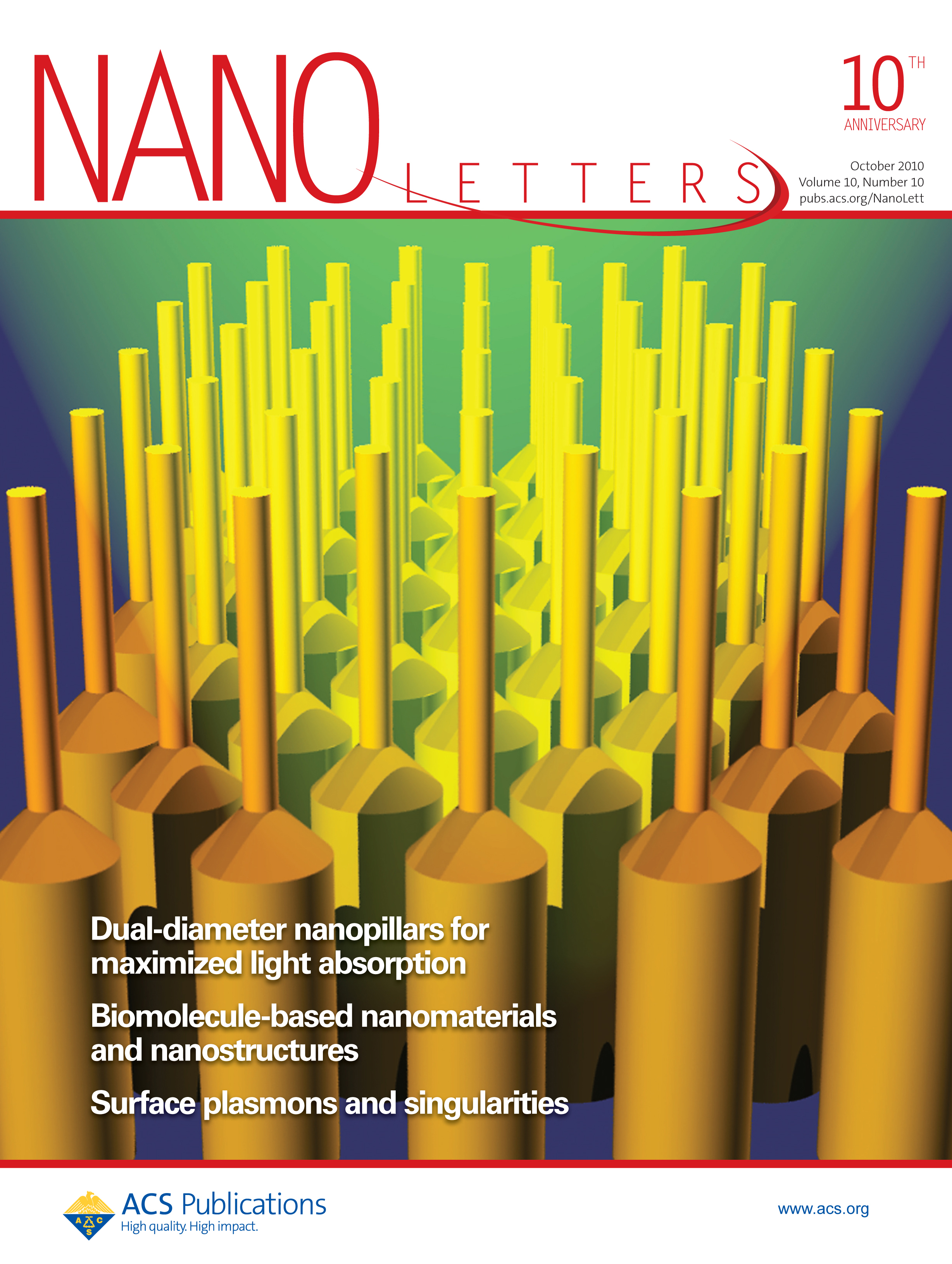

|


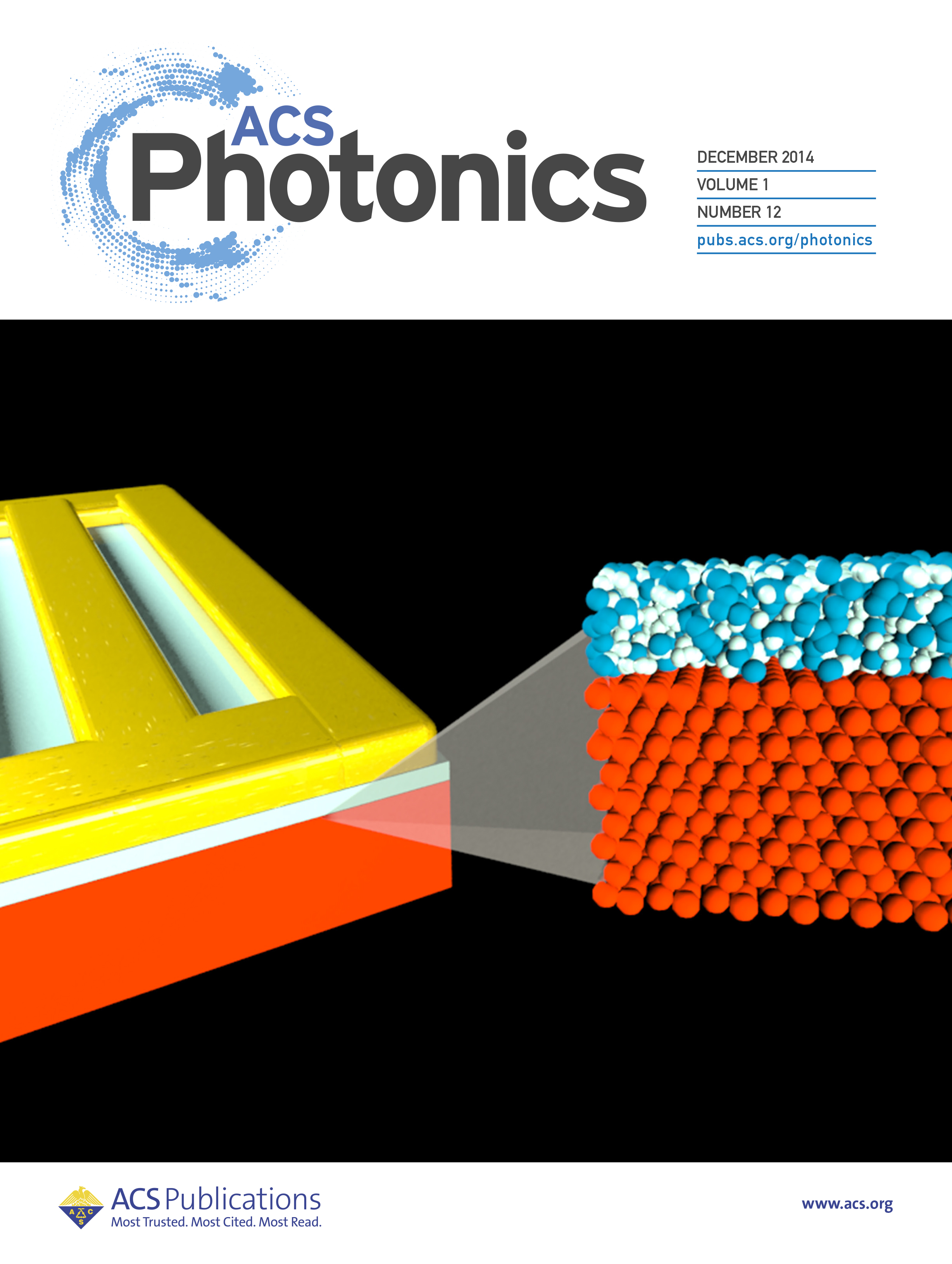