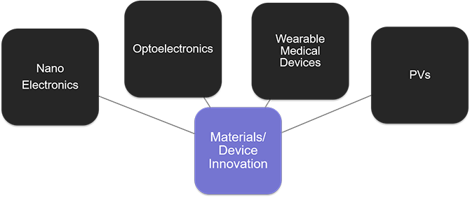
Our
research efforts focus on materials and device innovation for various
applications. Our research expands both technology development
(including materials, processing, devices, systems) and fundamental
materials physics. Below are a few examples of past/current project
highlights.
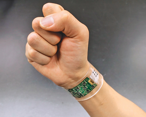
Wearable sweat analyzers for non-invasive medical and diagnostic devices.
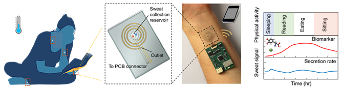
• Developed a portfolio of wearable sensors that are capable of
continuously analyzing the composition and flow rate of sweat for
non-invasive medical and diagnostic devices (Nature 2016; PNAS 2017; Nature Electronics 2018; Science Advances 2019; Science Advances 2020; Nature Comm 2021).
• The sensors can operate even when the subjects are at
near rest, where sweat rates are low, without the use of any induction
mechanism (Nature Comm, 2021).
• Able to detect cystic fibrosis patients through Cl- and Na+ concentration measurements using wearable bands (PNAS 2017). We observed strong regulation of ions in sweat, including pH, Cl- and Na+ (Nature 2016; Science Advances 2019). We observed strong correlation of vitamin C (Advanced Materials, 2021), nicotine (ACS Sensors, 2020), caffeine (Advanced Materials, 2018) and levodopa levels (Nano Letters,
2019) in sweat to intake, and were able to measure the absorption and
metabolism rates. We showed a strong correlation between local sweat
rate measurements and whole body weight loss (Science Advances 2019), and have observed a strong dependence of sweat rate on mental stress (Nature Comm, 2021).
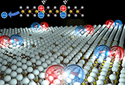
2D Optoelectronics: Quantum of absorbance, interlayer excitons in vdW heterostructures, and perfectly bright monolayers.
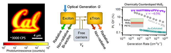
• Demonstrated near-unity photoluminescence quantum yield in TMDC monolayers at all exciton concentrations.
Specifically, neutral exciton recombination at low exciton
concentrations is entirely radiative (Science 2019, Science
2015) as observed by moving the Fermi level near mid-gap. At high
exciton concentrations, nonradiative exciton-exciton annihilation is
eliminated by applying a small mechanical strain to favorably tune the
band structure (Science 2021).
• Reported molecular monolayers with near-unity
photoluminescence quantum yield with a lifetime of 10’s of psec. This
material could result in the development of the fastest LEDs (Nature Comm, 2019; Matter 2020).
• Developed actively variable mid-IR LEDs and
photodetectors based on black phosphorous. A single device can be
actively tuned to operate between 0.22 to 0.53 eV by reversible
application of strain, taking advantage of the extraordinary
sensitivity of black phosphorous bandgap to strain. (Nature 2021).
• Measured the quantum unit of absorbance in 2D semiconductors (PNAS,
2013). The magnitude of absorption associated with each interband
transition in a 2D semiconductor (non-excitonic system) is ~1.6%,
independent of material thickness or other fundamental material
properties. The total absorption is thus dictated by the total number
of allowed interband transitions.
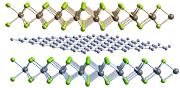
• First report of spatially indirect emission (i.e., spatially indirect excitons) in van der Waals heterobilayers (PNAS 2014).
Ultimate scaling limit of FETs
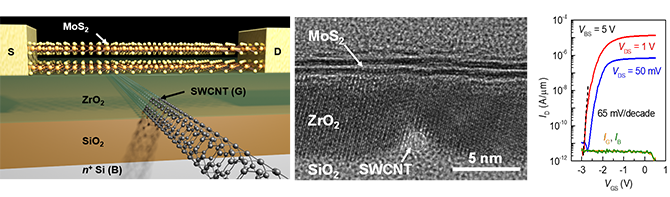
• Demonstrated 1nm physical gate length transistors with near-ideal switching performance (Science
2016). The heavier effective mass and lower dielectric constant
combined with atomically thin and uniform thickness, and naturally
passivated surfaces of MoS2 provided advantages over silicon in FET
scaling. The work highlights the key material and device properties
that need to be carefully considered in the design of future nanoscale
transistors.
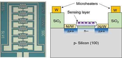
Silicon FET based gas sensors (CS-FETs)
• Demonstrated highly sensitive gas sensors based on bulk Si MOSFETs that are surface modified (Science Advances, 2017; ACS Nano, 2018, ACS Sensors 2019, Advanced Materials
2020). The gate electrode is replaced with a chemical sensing layer
whose work function changes selectively with gas exposure. The result
is a current modulation in the underlying Si MOSFET. Integrated
micro-heaters, operating slightly above the Dew point, mitigate ambient
humidity effects which was one of the fundamental challenges in the
field. With proper doping and electrostatics, ultrathin inversion
layers are generated in bulk MOSFETs, resulting in high sensitivity.
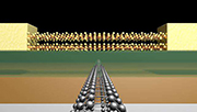
III-V nanosheet transistors on Silicon
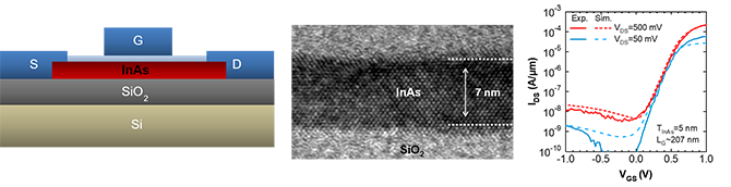
•
Developed ultrathin body III-V on insulator (XOI) device concept as a
platform for integrating high mobility III-V nanosheets (down to 3 nm in thickness) on Si for low
power electronics (Nature,
2010). Reported p- and n-type III-V FETs with high
mobilities and subthreshold swing
as low as ~70 mV/decade.
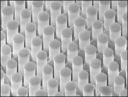
Low temperature growth of III-V crystals on amorphous substrates
• Developed a templated liquid phase growth process
for direct synthesis of single-crystalline III-V structures with user
defined geometry and topography on virtually any substrate (Nature Comm
2016), without the need for lattice matching constraints. The growth
can be performed at low substrate temperatures, down to 180C, making it
compatible with plastics, glass and Si CMOS (PNAS 2020).
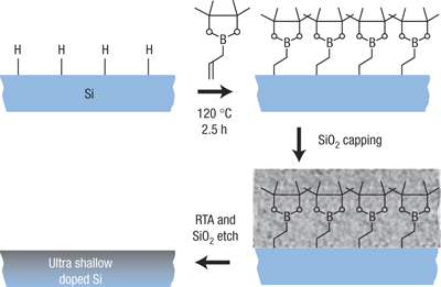
Monolayer Doping
•
Developed monolayer doping (MLD) for ultrashallow junctions. The process
utilizes self-assembled monolayers of dopant containing species on
semiconductor surfaces (including Si, Ge and III-V’s), followed by
formation of a silicon dioxide cap and subsequent diffusion by thermal
annealing (Nature Materials, 2008; Nano Letters,
2009). The process yielded the shallowest junctions reported at
the time in silicon, down to ~3 nm in thickness. It demonstrated that
surface diffusion can be tuned to achieve ultrashallow junctions
without sacrificing dopant dose uniformity. The dopant containing
monolayers can be formed using a half-cycle of an ALD process (ACS Applied Materials & Interfaces,
2017). A polymer-based counterpart of the process was also developed,
which, for example, could be used for printing dopant speciess for Si
PVs to eliminate expensive photolithography steps (The Journal of Physical Chemistry Letters, 2013).
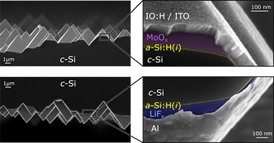
Dopant Free Silicon Solar Cells
•
Demonstrated a dopant-free Si solar cell concept with all fabrication
processes performed at near room temperature (Nature Energy 2016; Advanced Energy Materials 2019; ACS Energy Letters 2018; Nature Energy 2019).
We utilized extremely low work function (e.g., LiF) and high work
function (e.g., MoOx) materials as electron and hole contacts,
respectively without the need for heavily doped regions. Solar cells
with efficiencies >23% have now been reported based on this device
architecture.
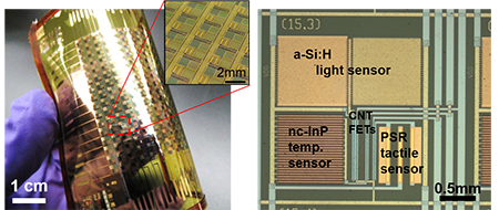
Electronic Skin
- Demonstrated
heterogenous integration of differnet electronic, sensing, and display
components based on different material classes on thin plastic substrates that could wrap around different
surfaces (Nature Materials 2010; Nature Materials
2013). From an engineering standpoint, human skin acts as our interface
with the environment. The goal of this research program on electronic
skin (e-skin) was to develop thin, flexible substrates that mimic
certain properties of human skin, and enable a new form of
human-machine interfacing. In essence, e-skin consists of mechanically
flexible sensor networks that can wrap irregular surfaces, and
spatially map and quantify various stimuli.