Solar energy
represents one of the most abundant and yet
least harvested sources of renewable energy. In recent
years,
tremendous progress has been made in developing solar devices that can
be
potentially mass employed with costs approaching and in some cases
surpassing
grid parity. Future research requires development of new material
systems
and device concepts that simultaneously offer high efficiencies and low
processing costs. In this regard, our group has made a number of major
advancements, including:
(i)
Development
of a new thin film growth mode for the growth of ultra-large
grain III-V semiconductor thin films on amorphous substrates with
optoelectronic properties approaching those of epitaxially grown,
single-crystal
layers (Scientific Reports, 2013;
Nature Comm, 2016).
(ii)
Development
of high efficiency dopant free asymmetric heterocontact (DASH) silicon
solar cells with all fabrication process steps performed near room
temperature and cell efficiencies >20% (Nature Energy, 2016).
(iii)
Demonstration of the highest
efficiency photocathodes for sunlight to fuel conversion
using nanotextured InP (Angew. Chem. Int. Ed., 2012).
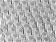
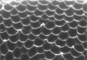
1.
New
growth mechanisms for non-epitaxial III-V photovoltaic devices
III-V
semiconductors have exhibited
the highest conversion efficiencies for solar cell devices to-date.
However,
their high costs, mainly associated with (i) the use of expensive
single
crystalline growth substrates and (ii) inefficient growth techniques
with low
material utilization yields and expensive precursors have prevented
their
large-scale use. To address these limitations, our group has
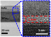
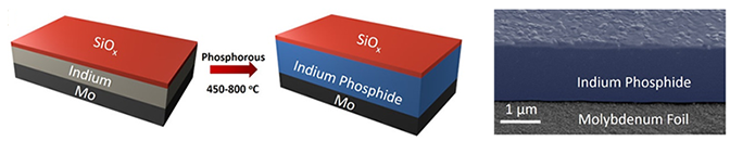
recently
demonstrated a thin-film vapor-liquid-solid (TF-VLS) growth mode which
enables
micron thick thin films with average grain sizes exceeding 100 microns (R. Kapadia, Z. Yu et al. Scientific
Reports, 2013). The TF-VLS process has been implemented on
insulators and
metal films alike, and provides excellent materials utilization. The
projected
efficiencies of these cells, in the absence of parasitic contributions
not
fully optimized in the lab setting, can surpass 20% in our thin-film
geometry
with high materials. The process
has also been extended to the direct growth of single cyrstalline
patterns on amorphous substrates (K.
Chen, R. Kapadia, et al., Nature Comm,
2016).
2.
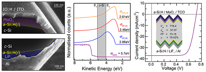
Dopant
free carrier selective contacts
In
crystalline silicon solar cells,
electron and holes are separated by either diffusing dopants into or
depositing
doped layers onto the two surfaces of the silicon wafer. Even with the
well-proven efficacy of this approach, device performance can be
limited via
optoelectronic losses and technological issues associated with high
temperature
processing etc. An alternative to this approach is to instead use
selective
materials such as metal oxides or alkaline metal fluorides which
achieve the
same functionality without the same losses. These advancements have led
to the
development of high efficiency dopant free asymmetric heterocontact
(DASH) silicon
solar cells, the first of their kind to demonstrate competitiveness
with
conventional processes (J. Bullock, Nature
Energy, 2016).
3.
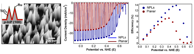
High
efficiency sun light to fuel conversion
In
addition to the solar cell related
activities, our group is actively engaged in
developing
efficient photoelectrochemical (PEC) cells that convert sun light to
fuel
(e.g., hydrogen). Specifically, our group
holds the highest efficiency photocathode based on a single
absorber material by using nanotextured InP (M.H. Lee, et al, Angew.
Chem.,
2012) for water splitting. We have
shown
that by properly
texturing the
surface of InP to control the surface wetting, the surface bubble
formation
during fuel generation is drastically reduced which is often a limiting
factor in the performance of PEC cells. In
addition, we have shown surface
texturing to be essential in a PEC
cell for antireflective (AR) properties given that conventional AR
coating
cannot be used since the semiconductor needs to be in direct contact
with the
electrolyte. As a result, a drastic
improvement in the performance of InP PEC cells is demonstrated by
nanotexturing the surface, thereby, enabling our group to demonstrate
the
highest performing photocathode reported to date. Although not as
mature as solar cells, PEC devices present yet another platform for
harvesting solar
energy and
present tremendous research opportunities moving forward by properly
engineering materials and devices to enhance the conversion
efficiencies of the
photoelectrodes. This project presents an excellent example of
interfacing
chemistry with device physics by using materials innovation as a bridge.