|
|
|
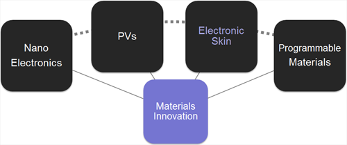
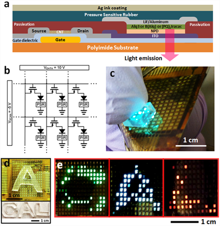
Electronic
Skin:
large-area sensor networks
From an
engineering
standpoint, human skin acts as our interface with the environment. The
goal of our research program on electronic skin (e-skin) is to develop
thin, flexible substrates that mimic certain properties of human skin,
and enable a new form of human-machine interfacing. In essence, e-skin consists of
mechanically flexible sensor networks
that can
wrap irregular surfaces, and spatially map and quantify
various
stimuli (example: Nature
Materials,
9, 821–826, 2010; Nature Materials,
2013, in press). Our long term vision is to heterogeneously integrate
a
wide range of sensor networks (e.g., pressure, strain, light,
temperature, and
humidity)
and associated electronics on large-area plastic substrates using
process
schemes that are compatible with conventional Si or LCD manufacturing
lines. In parallel, we are exploring printing
technologies for the fabrication of the envisioned systems. The
sensor elements are
based on a-Si, oxides, metals, piezoelectrics, and/or organic materials
that
are
processed
at <350 °C.
The
resulting e-skin may find
a
wide range
of applications in interactive
input/control devices, smart wallpapers,
robotics and medical/health monitoring devices. Towards
achieving this
long-term goal, most recently we have demonstrated a prototype e-skin
device that
not only spatially maps the applied pressure but also provides
instantaneous
response through a built-in active-matrix organic light-emitting diode
(AMOLED)
display. In
this system, OLEDs are turned on
locally where the surface is
touched, and the emitted light intensity quantifies the magnitude of
the
applied pressure. This work represents a “system-on-plastic”
demonstration
where various organic and inorganic materials, and three distinct
electronic
components – TFT, pressure sensor, and OLED arrays - are monolithically
integrated over large-areas on a single plastic substrate (Nature
Materials, 2013, in press). This project spans
surface
chemistry,
materials
processing, device design and process technology, circuit design and
systems integration.
|
|
Copyright ©
University of
California at Berkeley
|
|
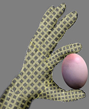
Artificial electronic-skin
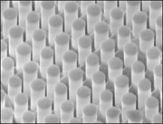
Nanopillars on metal foil
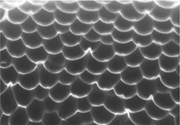
Roll-2-roll nanotextured Al
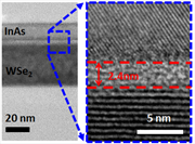
WSe2/InAs van der Waals heterojunctions
Printed nanowire arrays
|