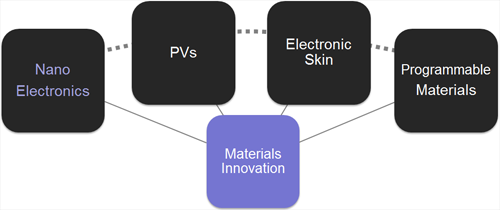
 Nanoelectronics
The
focus of
this research thrust is to develop
new devices/materials and related process technologies for
future low
power
electronics. Power efficiencies at both
device and circuit levels represent areas where important innovations
and advancements are needed for improving the overall performance of
ICs. We have made a
number of important advancements in this direction, ranging from those
that can
be readily adopted by industry to those that are longer-term and
currently remain
in pure research stage. A few examples of our recent contributions are
listed
below.
1.
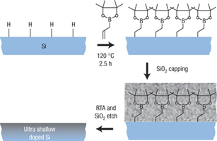
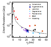
Monolayer Doping
Formation of
ultrashallow junctions (sub-5nm) that are defect free with high carrier
concentrations is essential for the source/drain contacts of future
nanoscale
devices. In
this regard, ion implantation has made significant progress in
obtaining shallower
junctions, but to-date obtaining high quality sub-5nm junctions with
implantion
has been challenging. Motivated by this
challenge, our group has developed a new
doping concept named monolayer doping
(MLD). In this approach, the semiconductor surface is
first conformally covered with a self-assembled monolayer of
dopant containing species using a self-terminating process (Nature Materials,
2008; Nano
Letters, 2009). The
dopant
atoms are subsequently incoraporated into the semiconductor using a
thermal
anneal step. Using this process, we have
demonstrated sub 5-nm junctions with low leakage currents, high dopant
activation rates, and high carrier concentrations. We
have shown the compatibility of the
process
for a wide range of dopants, and semiconductors (including Si, InAs,
and InP - both planar and 3D)
using appropriate surface chemistries (APL
2009, APL 2011). We
have transferred the technology to SEMATECH
which has used MLD to fabricate Fin-FETs, demonstrating
improved
transistor performance over similar devices fabricated by ion
implantation
(reported at IEDM, 2011). A
number of semiconductor companies have
adopted MLD for internal R&D. Moving
forward, besides the IC industry,
this
technology could also be used by the PV and LED industries. The project
demonstrates an elegant use of surface chemistry in making an important
advance
in device applications and process technologies.
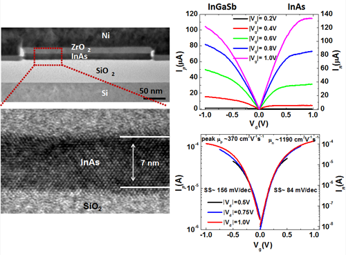
2. X-on-Insulator
(XOI)
One
approach for lowering the operating voltage of MOSFETs is to replace
the Si channel material with a thin layer of high mobility
semiconductor, such as III-V compound semiconductors. From
manufacturing point of view, it is desirable to still use Si as the
handling wafer due to its well established process technology, and
superb mechanical and thermal properties. Integration of high mobility
materials on Si, however, is challenging due to the large-lattice
mismatch. Two promising processes have been proposed, one
involving direct growth of III-V’s on Si using multiple buffer layers,
and the other, which was led by our group is based on layer transfer
(e.g., wafer bonding) of ultrathin III-V layers. We have named
the latter approach X-on-insulator
(XOI), analogous to conventional SOI (Nature,
2010; Nano Letters, 2011; APL, 2011; EDL, 2011, Nano Letters,
2012; Nano Letters, 2012; APL, 2012). To date, our
group has shown some of the highest performance III-V MOSFETs (both n-
and p-type) on Si substrates using
the XOI
geometry with channel thickness down to 3 nm. Specifically,
we have reported peak
effective mobilities of 1000-5000 cm2/Vs
depending on the thickness by using InAs XOI, with a subthreshold swing
of ~72
mV/decade and high interfacial quality.
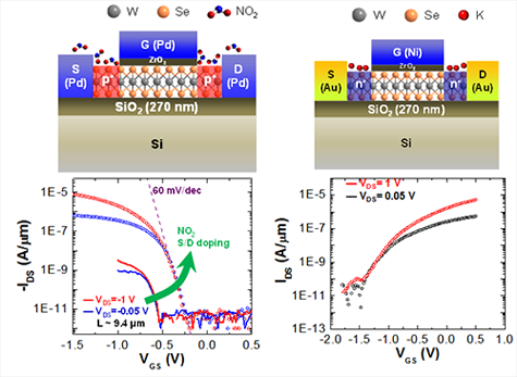
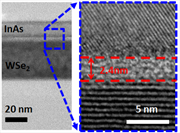
We have further
extended the work to the use of
layered chalcogenides as the “X”
layer. Chalcogenides are a new class of semiconductor
materials that can be made down to a single monolayer with large band
gaps,
minimal to no dangling bonds, and no native oxides. We are currently
examining
chemical
doping, heterjunctions, transport physics, and large-area growth of
various
layered chalcogenides, including WSe2. Particularly, our
group has demonstrated for the first
time that few-layer and monolayer
WSe2 can be selectively doped with electrons
and holes using surface charge transfer process, enabling n- and p-
MOSFETs with near identical electron and hole mobilities (Nano
Letters, 2012; Nano Letters,
2013). We have also explored chalcogenide heterostructures,
demonstrating that near ideal
electrical junctions can be obtained with van der Waals interfaces
(APL, 2013 - cover article).
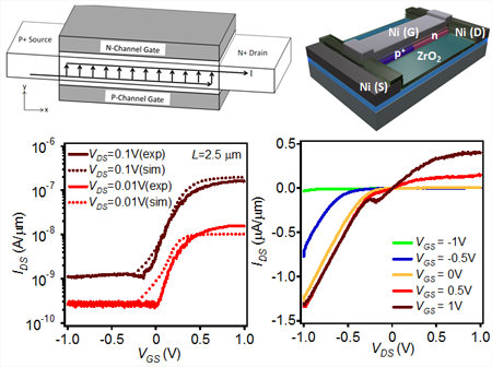
3. New
mV
Switch
The
operating
voltage of an ideal MOSFET, even with a high mobility material, cannot
be
scaled below ~300 mV given the theoretical substreshold swing of 60
mV/decade. In this regard, developing a
switch that can operate at voltages <300 mV is of fundamental
and
practical importance. Our group has been
exploring a number of alternative switching mechanisms, including
band-to-band tunneling
(i.e., TFETs) based on variety of material
systems with engineered band-alignments. We are focusing on using
III-V, III-N, chalcogenides and
oxides,
configured into proper heterostructures for exploiting new switching
mechanisms. One example includes ultrathin-body XOI TFETs (APL, 98, 113105, 2011).
|